EasyEDA Document Format
EasyEDA Document Format
Common Information
EasyEDA is a free, zero-install, Web and cloud-based EDA tool suite, integrating powerful schematic capture, mixed-mode circuit simulation and PCB layout.
EasyEDA team tries to make our users happy. We provide an open ASCII file format. With this file format, you can create a schematic or PCB using some codes, even with Notepad. When you try to add hundreds of LEDs to a schematic or PCB batch, you will find out that you can use codes to create an EasyEDA file, then import it to EasyEDA. It is fun and quick.
EasyEDA's file is a JSON file, but we compress all of the shape's attributes to a simple string, which will make the file size smaller and saving to server faster. More importantly, with this solution you can create some very big designs. Most browsers will crash when trying to decode the big JSON files. But EasyEDA will provide an API to let you to access the EasyEDA friendly JSON object, so you can hack the designs in the EasyEDA editor.
Ok, let's explain them with examples.
Example
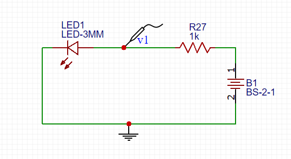
Schematic Example
Schematic JSON File Source
check it via github gist Schematic json
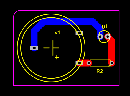
PCB Example
PCB JSON File Source
check it via github gist PCB json
General File Struct
Delimiter Mark
From the above JSON source, you can find there are lots of `, ~, ^^ and #@$ characters. These characters are used as delimiter mark. These characters are not used frequently in design.
Note: Although these characters were not picked properly at the very beginning, we can't change these, EasyEDA already has lots of existing designs
~ (Tilde)
~ is used to separate the attributes of the shapes. Taking rectangle as an example. R~170~100~10~10~200~130~#99FF00~1~0~none~gge36~, when use pure JSON file, it should be look like below, check it via github gist rect json.
So EasyEDA's source is small in file size and will transfer from the internet faster.
`(Back Quote)
` is used to separate the custom attributes.
package`LED3MM stands package:LED3MM
^^(Double Circumflex)
^^ is used to join segments, just used in netFlag , Pin and pAD.
#@$(Octothorpe Ampersat Dollar)
Document Type
check it via github gist document type
Canvas Coordinates
The canvas is a two-dimensional grid. The upper-left corner of the canvas has the coordinate (0,0)
SVG
EasyEDA uses Scalable Vector Graphics (SVG) which is an XML-based vector image format for two-dimensional graphics to realize the shapes.
Q&A
1. How to check the json file format
Check the EasyEDA source dialog out, copy the text to text area, then click the Apply button. That is all.
EasyEDA Schematic File Format
Head
Head information for schematic and subckt.
"head":"1~1.7.5~Author`Dillon`~TRAN`2u`2m`0`{AC`dec``0`0`{DC`0``0`0`{TF``"
Format:
- document version:
1.7.5h - custom attributes: key: value pairs, separate with `, added via Add new parameter
 4. spice simulation configure store, Now can set four types
 tran, AC, DC, TF, every type split with {. When opening the simulation dialog, these information will be listed in like below image. 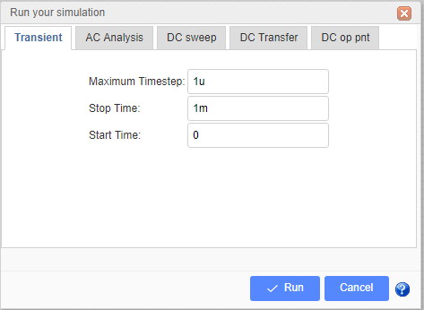
Head information for Schematic Symbol, Spice Symbol and Subpart
"head":"7~1.7.5~400~300~package`DIP08`nameDisplay`0`nameAlias`Model`Model`555`name`555`pre`U?`spicePre``Contributor`Dillon"
Format:
- document version:
1.7.5 - origin x position. Reserved field, can't be changeded
- origin y position. Reserved field, can't be changeded
- custom attributes: key: value pairs, separate with `, added via Add new parameter. package: DIP08nameDispaly: 0 (hide it is name when placed to schematic) nameAlias: Modelname:555pre:U? , when place to schematic, will be marked as U1, U2. subpart will be set as U?.1, U?.2 etc. spicePre:X, X stands for a subckt. sourceId:xxxxxxxxx (just for schematic Lib and spice symbol)
Place it to schematic canvas, it's attributes will be looked like below image. The name field is alias as Model and it is invisible. 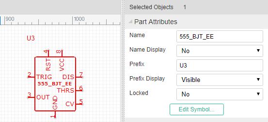
Canvas
"canvas":"CA~1200~1200~#FFFFFF~yes~#CCCCCC~10~1200~1200~line~10~pixel~5~400~300"
Format:
- command: CA
- view box width: 1200, View Box Width / Canvas width = scaleX
- view box height: 1200,View Box Height / Canvas Height = scaleY
- back ground: #FFFFFF
- grid visible: yes/none
- grid color: #CCCCCC
- grid size: 10 pixel
- canvas width: 1200 pixel
- canvas height: 1200 pixel
- grid style: line/dot
- snap size: 10 pixel
- unit: pixel(Always pixel)
- ALT snap size:5 (Snap Size when pressing the
ALTKey) - origin x position
- origin y position
Canvas setting image 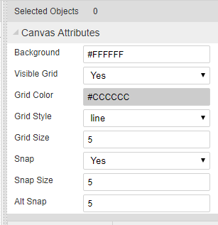
Shapes
The shape is an array. EasyEDA store various shape in this field, they are different with a command which locate at the begin of the string.
"shape":[
    "PL~210 100 260 100~#000000~2~0~none~gge58",
    "R~210~110~~~50~30~#000000~1~0~none~gge61",
    "I~90~90~271~105~0~https://easyeda.com/assets/static/images/logo-140x39.png~gge62",
    "PG~310 100 350 130 300 150 290 150 270 120~#000000~2~0~none~gge64",
    "PT~M230 170 C270 200 270 170 240 150 240 150 240 150 240 150~#000000~2~0~none~gge65"
]
Rectangle
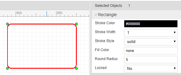
"R~650~0~20~20~230~160~#FF0000~2~1~#9966FF~gge5"
Format:
Check Rect element of SVG out.
- command: R
- x: 650
- y: 0
- rx: 20
- ry: 20
- width: 230
- height: 160
- strokeColor: #FF0000
- strokeWidth: 2 //pixel
- strokeStyle: 1
- fillColor: #9966FF
- id: gge36
- locked:null Rect's attributes and image looks like bellow image:
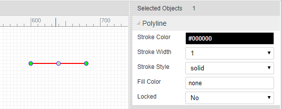
Polyline
"PL~610 130 780 130~#FF0000~5~0~none~gge6"
Format: Check Polyline element of SVG out.
- command: PL
- points: 610 130 780 130
- strokeColor: #FF0000
- strokeWidth: 5 //pixel
- strokeStyle: 0
- fillColor: none
- id: gge6
- locked:null Polyline's attributes and image looks like bellow image:
Path
"PT~M670 300 C830 370 850 230 920 300 920 300 920 300 920 300~#000000~1~0~none~gge17"
Format: Check Path element of SVG out.
- command: PT
- pathString:M670 300 C830 370 850 230 920 300 920 300 920 300 920 300
- strokeColor: #FF0000
- strokeWidth: 5 //pixel
- strokeStyle: 0
- fillColor: none
- id: gge6
- locked:null Path's attributes and image looks like bellow image:
 bezier is a path too.
Arc
"A~M 1020 60 A 80 80 0 0 1 953.096 199.904~968.78,121.45,1048.785,201.457,1018.785,61.457,948.785,221.45~#FF0000~3~0~none~gge19"
Format: Arc is a Path element, Check Path element of SVG out.
- command: A
- pathString:M670 300 C830 370 850 230 920 300 920 300 920 300 920 300
- helperDots: the four green dots
- strokeColor: #FF0000
- strokeWidth: 3 //pixel
- strokeStyle: 0
- fillColor: none
- id: gge19
- locked:null
ARC's attributes and image looks like bellow image:
Pie
"PI~M 970 40 L 1189.9 34.4509 A 220 180 0 0 1 923.103 215.863 Z~970,40,1190,220,1327.7106323242188,30.973068237304688,923.1032104492188,215.86282348632812~#FF0000~3~0~#CCCCCC~gge22"
Pie is a Path element, Check Path element of SVG out. Pie is similar with Arc, the pathString has a Z
- command: PI
- pathString:M 970 40 L 1189.9 34.4509 A 220 180 0 0 1 923.103 215.863 Z
- helperDots: the four green dots
- strokeColor: #FF0000
- strokeWidth: 3 //pixel
- strokeStyle: 0
- fillColor: none
- id: gge19
- locked:null
Pie's attributes and image looks like bellow image: 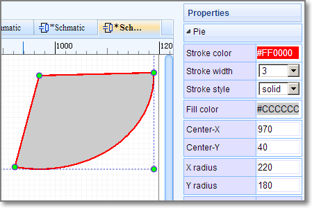
Bus Entry
"BE~0~660~150~670~140~gge15"
Format:
- command: BE
- rotation:0
- start x1: 660
- start y1: 150
- end x1: 670
- end y1: 140
- id: gge15
- locked:null
Bus Entry's attributes and image looks like bellow image: 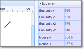
Image
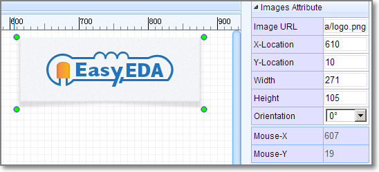
"I~610~10~271~105~0~https://easyeda.com/assets/static/images/logo-140x39.png~gge12"
Format: Check Image element of SVG out.
- command: I
- x: 610
- y: 10
- width: 271
- height: 105
- rotation: 0
- href:https://easyeda.com/assets/static/images/logo-140x39.png
- id: gge12
- locked:null Image's attributes and image looks like bellow image:
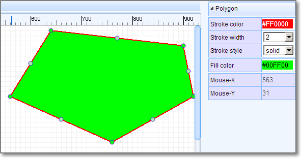
Polygon
"PG~640 10 900 40 920 140 760 230 560 140~#FF0000~2~0~#00FF00~gge10"
Format: Check Polygon element of SVG out.
- command: PG
- points: 640 10 900 40 920 140 760 230 560 140
- strokeColor: #FF0000
- strokeWidth: 2 //pixel
- strokeStyle: 0
- fillColor: #00FF00
- id: gge10
- locked:null Polygon's attributes and image looks like bellow image:
Line
"L~360~160~510~160~#FF0000~2~0~none~gge11"
Format: Check Line element of SVG out.
- command: L
- x1:360
- y1:160
- x2:510
- y2:160
- strokeColor: #FF0000
- strokeWidth: 2 //pixel
- strokeStyle: 0
- fillColor: #00FF00
- id: gge11
- locked:null
Circle
"C~710~170~105~#FF0000~2~0~#0000FF~gge12"
Format: Check Circle element of SVG out.
- command: C
- cx:720
- cy:90
- r:105
- strokeColor: #FF0000
- strokeWidth: 2 //pixel
- strokeStyle: 0
- fillColor: #0000FF
- id: gge12
- locked:null
Bus
"B~570 130 680 130 680 210~#008800~2~0~none~gge19"
Bus is similar with Polyline, Bus is start with B, polyline start with PL.
Pin
"P~show~0~1~670~30~~gge23^^670~30^^M 670 30 h -20~#880000^^1~648~33~0~1~end~~11pt^^1~655~29~0~1~start~~11pt^^0~653~30^^0~M 650 27 L 647 30 L 650 33"
Pin configure
P~show~0~1~670~30~~gge23- command: P
- display: show/'' (bad design, should use yes/none)
- electric: 0, can be ['Undefined', 'Input','Output','I/O','Power']
- spice pin number: 1
- position x: 670
- position y: 30
- rotation: null, can be ['null' or 0, '90', '180', '270']
- id: gge23
- locked: null
pin dot
670~30The gray dot at the end of the Pin, it is important.- pin dot x: 670
- pin dot y: 30
pin path
M 670 30 h -20~#880000- path: M 670 30 h -20, a 20 pixel horizontal line start from pin dot
- pin color: #880000
name
1~648~33~0~1~end~~11pt- visible : 1/0 stand show or hide
- position x: 648
- position y: 33
- rotation: 0
- text: 1
- text anchor: end
- font family: null, default is Verdana
- font size: 11pt, default is 7pt
number
1~655~29~0~1~start~~11ptthe same as name above
dot
0~653~30stands for not. a circle with radius in 3 pixel
- visible : 0/1 hide / show
- circle x: 653
- circle y: 30
clock
0~M 650 27 L 647 30 L 650 33- visible: 0/1 hide / show
- clock path: M 650 27 L 647 30 L 650 33
Pin's attributes and image looks like bellow image: 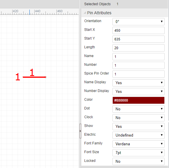
Ellipse
"E~720~90~105~65~#FF0000~2~0~#0000FF~gge12"
Format: Check Ellipse element of SVG out.
- command: E
- cx:720
- cy:90
- rx:105
- ry:65
- strokeColor: #FF0000
- strokeWidth: 2 //pixel
- strokeStyle: 0
- fillColor: #0000FF
- id: gge12
- locked:null
Ellipse's attributes and image looks like bellow image: 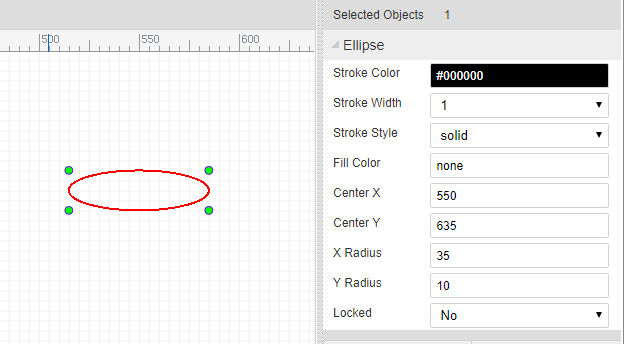
Arrowhead
"AR~part_arrowhead~1060~120~gge23~180~M 1060 120 L 1063 126 L 1055 120 L 1063 114 Z~#FF0000"
Format:
- command: AR
- part Type:part_arrowhead, not used
- x:1060
- y:120
- id:gge23
- rotation: 180
- path String: M 1060 120 L 1063 126 L 1055 120 L 1063 114 Z
- fillColor: #FF0000
- locked:null
Arrow head's attributes and image looks like bellow image:
Annotations
"T~L~540~60~0~#0000FF~~9pt~bold~normal~~comment~Text~1~start~gge26"
Check Text element of SVG out. Format:
- command: T
- mark: L //
L= label,N= Name,P= prefixN,Pare for Symbol - position x:540
- position y:60
- rotation:0
- fill color: #0000FF
- font family: null, default is Verdana
- font size: 9pt
- font-weight: bold
- font style: normal
- dominant baseline: null
- text type: comment // comment or spice command
- string: Text
- visible: 1/0 show/hide (use for mark
NorP) - text anchor: start (start middle end)
- id:gge26
- locked:null
Text's attributes and image looks like bellow image: 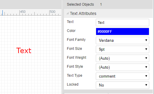
Netlabels
"N~360~100~0~#FF0000~VCC~gge32~start~362~100~Times New Roman~",
Format:
- command: N
- pin dot x: 360
- pin dot y: 100
- rotation: 0
- fill color: #FF0000
- name: VCC
- id: gge32
- text anchor: start (start middle end)
- postion x: 362
- postion y: 100
- font family: Times New Roman
- font size:null default is 7pt
- locked:null
netlabel's attributes and image looks like bellow image: 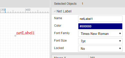
Netflags
Netflag is very similar with netlabel
"F~part_netLabel_gnD~330~110~~gge41^^330~110^^GND~#000080~319~97~0~start~0~Times New Roman~9pt^^PL~330 120 330 110~#000000~1~0~none~gge44^^PL~320 120 339 120~#000000~1~0~none~gge45^^PL~324 122 337 122~#000000~1~0~none~gge46^^PL~326 124 333 124~#000000~1~0~none~gge47^^PL~329 126 331 126~#000000~1~0~none~gge48",
configure
P~show~0~1~670~30~~gge23- command: F
- part id: part_netLabel_gnD
- position x: 330
- position y: 110
- rotation: null [0, 90, 180, 270]
- id: gge41,
- locked: null
pin dot
670~30The gray dot at the end of the Pin, it is important.- pin dot x: 330
- pin dot y: 140
mark string
GND~#000080~319~97~0~start~0~Times New Roman~9pt- net flag string: GND
- color: #000080
- position x: 319
- position y: 97
- rotation: 0 [0, 90, 180, 270]
- text anchor: start (start middle end)
- visible: 1/0 show/hide the net flag string
- font family: Times New Roman
- font size:null default is 7pt
shapes
All other items are shapes.
netflag's attributes and image looks like bellow image: 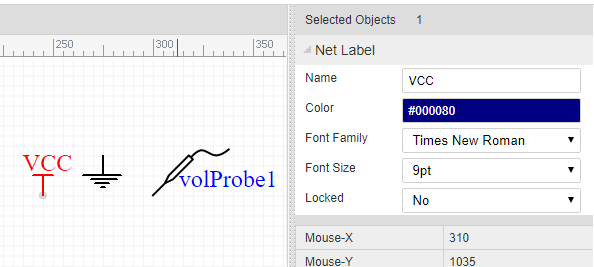
Wire
"W~570 130 680 130 680 210~#008800~2~0~none~gge19"
Wire is similar with Polyline, Wire is start with W, polyline start with PL.
Junctions
"J~420~140~2.5~#CC0000~gge18",
Format:
- command: J
- pin dot x: 420
- pin dot y: 140
- junction circle radius: 2.5 pixel
- fill color: #CC0000
- id: gge18
- locked:null
Junction's attributes and image looks like bellow image: 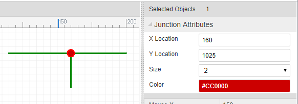
No Connect Flag
"O~960~410~gge5~M956,406 L964,414 M964,406 L956,414~#FF0000"
Format:
- command: O
- pin dot x: 960
- pin dot y: 410
- id: gge5
- pathStr: M956,406 L964,414 M964,406 L956,414
- color: #FF0000
- locked:null
No Connect Flag's attributes and image looks like bellow image: 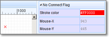
Symbol
"LIB~220~140~package`C1`nameAlias`Value(F)`Value(F)`1u`spicePre`C`spiceSymbolName`Capacitor`~~0~gge66#@$T~N~214~129~0~#000080~Arial~~~~~comment~1u~1~start~gge68#@$T~P~214~120~0~#000080~Arial~~~~~comment~C1~1~start~gge69#@$PL~218 148 218 132~#A00000~1~0~none~gge70#@$P~show~0~1~200~120~180~gge71^^200~140^^M 210 140 h -10~#800^^0~214~140~0~1~start~~^^0~206~136~0~1~end~~^^^^#@$PL~230 140 222 140~#A00000~1~0~none~gge72#@$PL~222 132 222 148~#A00000~1~0~none~gge73#@$P~show~0~2~210~120~0~gge74^^240~140^^M 230 140 h 10~#800^^0~226~140~0~2~end~~^^0~234~136~0~2~start~~^^^^#@$PL~218 140 210 140~#A00000~1~0~none~gge75"
configure
LIB~270~140~package`DO35-7`nameAlias`Model`Model`1N4001`spicePre`D`spiceSymbolName`Diode`~~0~gge116- command: LIB
- position x: 270
- position y: 140
- rotation: 0, can be ['null' or 0, '90', '180', '270']
- import flag: 0 just used in import from eagle
- id: gge116
- locked: null
shapes
All other items are shapes.
strokeStyle
- 0 : solid
- 1 : dashed
- 2 : dotted
Q&A
1. Why don't save the Wire, Annotion, netlabel, netflag to Shape field.
These items will be used to create netlist, save them to separate field will make you spent more less time to do this. We don't need to traversal all the shapes.
EasyEDA PCB File Format
Head
Head information for PCB.
"head":"3~1.7.5~Author`Dillon`"
Format:
- document version:
1.7.5 - custom attributes: key: value pairs, separate with `, added via Add new parameter
Head information for PCB Footprint
"4~1.7.5~400~300~`pre`U?`Contributor`Dillon"
Format:
- document version:
1.7.5 - origin x position. Reserved field, can't be changeded
- origin y position. Reserved field, can't be changeded
- custom attributes: key: value pairs, separate with `, added via Add new parameter.
pre:U? , when place to PCB, will be marked as U1, U2. Contributor:DillonsourceId:xxxxxxxxx (just for Footprint)
Parameters Dimensions
EasyEDA support millimeter, inch and millimeter, but when these items are stored to a file, all of them will be expressed as 10X mil. Taking line lengths or widths for examples, stroke width equal 1, stands 10mil.
Canvas
"CA~2400~2400~#000000~yes~#FFFFFF~10~1200~1200~line~1~mil~1~45~visible~0.5~400~300"
Format:
- command: CA
- view box width: 2400(24000 mil), View Box Width / Canvas width = scaleX = 2
- view box height: 2400(24000 mil),View Box Height / Canvas Height = scaleY = 2
- back ground: #000000
- grid visible: yes/none
- grid color: #FFFFFF
- grid size: 10(100 mil)
- canvas width: 1200 (12000 mil)
- canvas height: 1200 (12000 mil)
- grid style: line/dot
- snap size: 1 (10 mil)
- unit: mil(inch, mil, mm)
- routing width: 1 (10mil)
- routing angle: 45 degree( 45 90 free)
- copper area: visible/invisible
- ALT snap size: 0.5 ( 5 mil Snap Size when pressing the
ALTKey) - origin x position
- origin y position
Canvas setting image 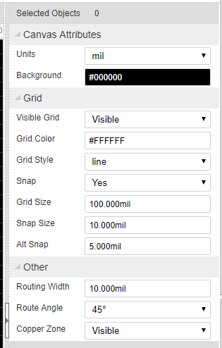
System Color
"#000000~#FFFFFF~#FFFFFF~#000000~#FFFFFF"
Format:
- future use: #000000
- future use: #FFFFFF
- future use: #FFFFFF
- hole Color: #000000
- DRC error: #FFFFFF
Layers config
layers is an array, each layer is an item of the layers.
 "layers":[
    "1~TopLayer~#FF0000~true~true~true",
    "2~BottomLayer~#0000FF~true~false~true",
    "3~TopSilkLayer~#FFFF00~true~false~true",
    "4~BottomSilkLayer~#808000~true~false~true",
    "5~TopPasterLayer~#808080~false~false~false",
    "6~BottomPasterLayer~#800000~false~false~false",
    "7~TopSolderLayer~#800080~false~false~false",
    "8~BottomSolderLayer~#AA00FF~false~false~false",
    "9~Ratlines~#6464FF~true~false~true",
    "10~BoardOutline~#FF00FF~true~false~true",
    "11~Multi-Layer~#C0C0C0~true~false~true",
    "12~Document~#FFFFFF~true~false~true",
    "21~Inner1~#800000~false~false~false",
    "22~Inner2~#008000~false~false~false",
    "23~Inner3~#00FF00~false~false~false",
    "24~Inner4~#000080~false~false~false"
]
Format:
- layer id: 1
- layer name: TopLayer
- layer color: #FF0000
- visible: true, hints the objects in this layer show or hide
- active: false. active layer
- config: true. if be set false, you can't see it on the layer toolbar.
Preference
"preference":{
    "hideFootprints":"gge118~gge221~gge227~gge233",
    "hideNets":"BSYNC~DREQ~GPIO0~MICP~GND"
}
hideFootprints : when the id of the footprints in here, you can't see them on canvas. hideNets : when the net name in here, you can't see them on canvas, you can hide the ratline at here too. There are some guys would like to hide then GND ratline, then use copper area to connect all the GND pad.
DRC Rule
 "DRCRULE":{
    "trackWidth":0.7,
    "track2Track":0.7,
    "pad2Pad":0.8,
    "track2Pad":0.8,
    "hole2Hole":1,
    "holeSize":1.6
}
trackWidth: 0.7 (7 mil) track width track2Track: 0.7 (7 mil) track to track distance pad2Pad: 0.8(8 mil) pad to pad distance track2Pad: 0.8(8 mil) track to pad distance hole2Hole: 1(10 mil) hole to hole distance holeSize: 1.6(16 mil) hole diameter
This is a simple DRC, more later.
Shapes
The shape is an array. EasyEDA store various shape in this field, they are different with a command which locate at the begin of the string.
"shape":[
    "TRACK~1~1~S$19~311 175 351 175 352 174~gge18",
    "PAD~ELLIPSE~329~185~6~6~11~~1~1.8~~0~gge20",
    "VIA~329~202~3.2~~0.8~gge23",
    "COPPERAREA~2px~1~GND~349 247 492 261 457 314 339 329~1~solid~gge27~spoke~none~[]",
    "SOLIDREGION~1~~350 146 483 146 447 228 371 220~solid~gge26"
]
Unit
EasyEDA takes 10 mil as a basic factor, when a stroke width is 1, we can take it as 1*10mil = 10mil, is 2, we can take it as 2*10mil = 20mil
TRACK
"TRACK~1~1~S$19~311 175 351 175 352 174~gge18"
Format: Check Polyline element of SVG out.
- command: TRACK
- stroke Width: 1 (10 mil)
- layer id: 1 (TopLayer)
- net: "S$19"
- points: 311 175 351 175 352 174
- id : gge18
- locked: null
TRACK's attributes and image looks like bellow image: 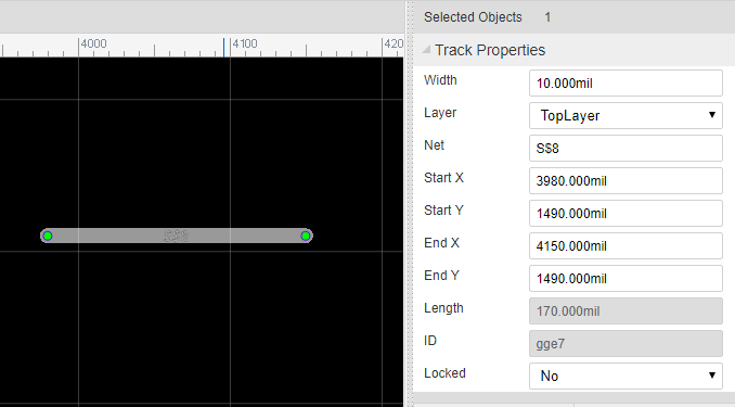
COPPERAREA
"COPPERAREA~2px~1~GND~349 247 492 261 457 314 339 329~1~solid~gge27~spoke~yes~[[\"M339,329 349,247 492,261 457,314z\"]]"
Format:
- command: COPPERAREA
- stroke Width: 2 (20 mil)
- layer id: 1 (TopLayer)
- net: GND
- points: 349 247 492 261 457 314 339 329
- clearance Width : 1 (10 mil)
- fill style: solid/none
- id: gge27
- thermal: spoke/direct
- keep island: none/yes
- copper zone: [["M339,329 349,247 492,261 457,314z"]] rings and holes
- locked: null
COPPERAREA's attributes and image looks like bellow image: 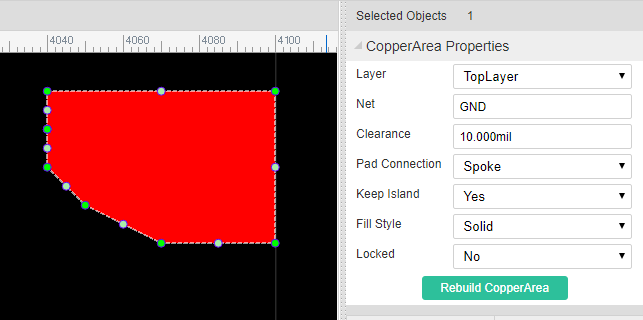
RECT
"RECT~406~220~105~52~1~gge32"
Format:
Check Rect element of SVG out.
- command: RECT
- x: 406
- y: 220
- width: 105
- height: 52
- layer id:1
- id: gge36
- locked:null
Rect's attributes and image looks like bellow image:
CIRCLE
"CIRCLE~363~273~42~1~3~gge33"
Format: Check Circle element of SVG out.
- command: CIRCLE
- cx:363 (3630 mil)
- cy:273
- r:42 (420 mil)
- stroke width: 1 (10mil)
- layer id: 3 (Top silk layer)
- id: gge33
- locked:null
CIRCLE's attributes and image looks like bellow image: 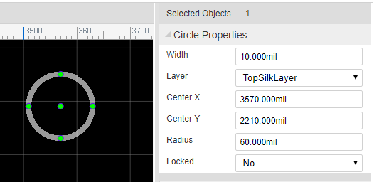
SOLIDREGION
"SOLIDREGION~1~GND~322 256 376 317 447 250 353 231~solid~gge34"
Format:
- command: SOLIDREGION
- layer id: 1 (Toplayer)
- net: GND
- points:322 256 376 317 447 250 353 231
- type: solid/cutout/npth
- id: gge34
- locked:null
SOLIDREGION's attributes and image looks like bellow image: 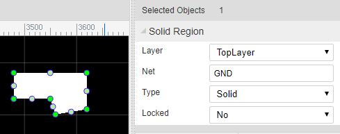
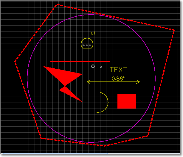
TEXT
"TEXT~L~351~252~0.8~0~none~1~~8~TEXT~M 352.55 250.64 L 352.55 258.27 M 350 250.64 L 355.09 250.64 M 357.49 250.64 L 357.49 258.27 M 357.49 250.64 L 362.22 250.64 M 357.49 254.27 L 360.4 254.27 M 357.49 258.27 L 362.22 258.27 M 364.62 250.64 L 369.71 258.27 M 369.71 250.64 L 364.62 258.27 M 374.65 250.64 L 374.65 258.27 M 372.11 250.64 L 377.2 250.64~~gge35"
Format:
- command: TEXT
- type: L/P (L = label, P = prefix)
- position x: 351 (3510 mil)
- position y: 252 (2520 mil)
- stroke width: 0.8 (8 mil)
- rotation: 0
- mirror : none ( not user now)
- layer id: 1 (Toplayer)
- net: ''
- font size: 8 (80 mil in height)
- string: TEXT
- text path: M 352.55 250.64 L 352.55 258.27 M 350 250.64 L 355.09 250.64 M 357.49 250.64 L 357.49 258.27 M 357.49 250.64 L 362.22 250.64 M 357.49 254.27 L 360.4 254.27 M 357.49 258.27 L 362.22 258.27 M 364.62 250.64 L 369.71 258.27 M 369.71 250.64 L 364.62 258.27 M 374.65 250.64 L 374.65 258.27 M 372.11 250.64 L 377.2 250.64
- display: '' (none = hide, other = show)
- id: gge35
- locked: null
TEXT's attributes and image looks like bellow image: 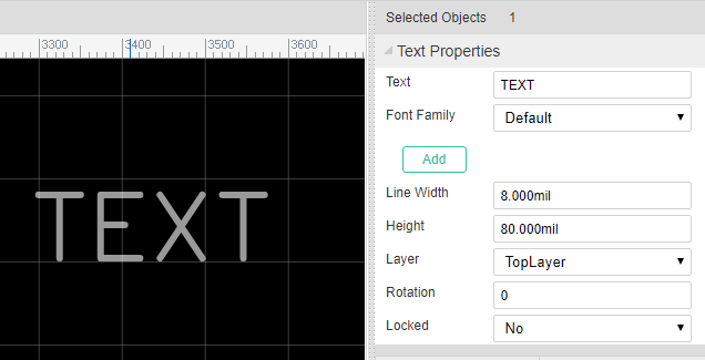
Arc
"ARC~1~1~S$51~M329,274 A26.95,26.95 0 0 1 370,309~~gge50"
Format: Arc is a Path element, Check Path element of SVG out.
- command: ARC
- stroke width: 1 (10 mil)
- layer id: 1 (Toplayer)
- net: S$51
- path string: M329,274 A26.95,26.95 0 0 1 370,309
- helper dots: the four green dots, no need in PCB, keep it blank
- id: gge19
- locked:null
ARC's attributes and image looks like bellow image:
PAD
"PAD~OVAL~814~371~6~16~11~~1~1.8~814 366 814 376~0~gge5~11~814 374.7 814 367.3~N"
Format:
- command: PAD
- shape: ELLIPSE/RECT/OVAL/POLYGON
- center x: 814
- center y: 371
- width: 6 (60 mil)
- height: 16 (160 mil)
- layer id: 11 (All)
- net: ''
- number: 1
- hole radius: 1.8 (18 mil)
- points: '' (ELLIPSE = '', RECT = outline points)
- rotation: 0 [0 - 360]
- id: gge19
- Hole(Length): 11 (110mil)
- Hole Points: 814 374.7 814 367.3 // slot hole from to point
- Plated:Y/N
- locked:null
PAD's attributes and image looks like bellow image: 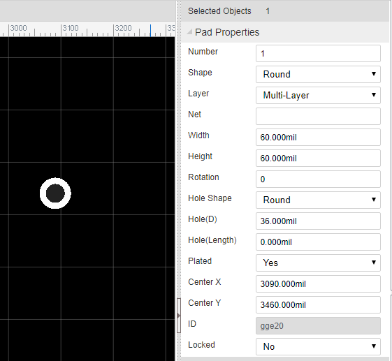
VIA
"VIA~432~215~3.2~~0.8~gge5"
Format:
- command: VIA
- center x: 432
- center y: 215
- diameter: 3.2
- net : ''
- hole radius: 0.8 (8 mil)
- id: gge5
- locked:null
VIA's attributes and image looks like bellow image: 
HOLE
"HOLE~284~255~4~gge5"
Format:
- command: HOLE
- center x: 284
- center y: 255
- diameter: 4
- id: gge5
- locked:null
HOLE's attributes and image looks like bellow image: 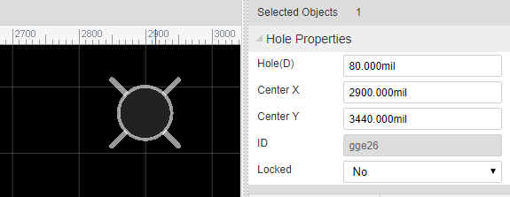
DIMENSION
"DIMENSION~3~M 301 217 L 442 217 M 306 220 L 301 217 L 306 214 M 437 220 L 442 217 L 437 214 M 369.5 209.82 L 370.05 209.55 L 370.86 208.73 L 370.86 214.45 M 372.94 213.09 L 372.66 213.36 L 372.94 213.64 L 373.21 213.36 L 372.94 213.09 M 377.74 208.73 L 375.01 212.55 L 379.1 212.55 M 377.74 208.73 L 377.74 214.45 M 380.9 209.82 L 381.45 209.55 L 382.26 208.73 L 382.26 214.45 M 384.06 208.73 L 384.06 210.64 M 386.25 208.73 L 386.25 210.64~gge8"
Format:
- command: DIMENSION
- layer id: 3 (Top Silk layer)
- path: M 301 217 L 442 217 M 306 220 L 301 217 L 306 214 M 437 220 L 442 217 L 437 214 M 369.5 209.82 L 370.05 209.55 L 370.86 208.73 L 370.86 214.45 M 372.94 213.09 L 372.66 213.36 L 372.94 213.64 L 373.21 213.36 L 372.94 213.09 M 377.74 208.73 L 375.01 212.55 L 379.1 212.55 M 377.74 208.73 L 377.74 214.45 M 380.9 209.82 L 381.45 209.55 L 382.26 208.73 L 382.26 214.45 M 384.06 208.73 L 384.06 210.64 M 386.25 208.73 L 386.25 210.64
- id: gge5
- locked:null
DIMENSION's attributes and image looks like bellow image:
DIMENSION just allows to change it layer id, if you don't accept this DIMENSION, delete it and redraw again.
Footprint
"LIB~245~240~package`CK17-B`~~~gge15~1#@$TEXT~P~295~219.5~0.7~0~~3~~4.5~C1~M 298.07 218.07L297.86 217.66 L297.45 217.25 L297.05 217.05 L296.23 217.05 L295.82 217.25 L295.41 217.66 L295.2 218.07 L295 218.68 L295 219.7 L295.2 220.32 L295.41 220.73 L295.82 221.14 L296.23 221.34 L297.05 221.34 L297.45 221.14 L297.86 220.73 L298.07 220.32 M 299.42 217.86L299.83 217.66 L300.44 217.05 L300.44 221.34 ~~gge16#@$TRACK~0.9~3~~257.5 224.5 332.5 224.5 332.5 255.5 257.5 255.5 257.5 224.5~gge17#@$PAD~ELLIPSE~245~240~9.4~9.4~11~~1~2.25~~0~gge18#@$PAD~ELLIPSE~345~240~9.4~9.4~11~~2~2.25~~0~gge19"
configure
LIB~245~240~package`CK17-B`~0~~gge15~1- command: LIB
- position x: 270
- position y: 140
- rotation: 0, can be [0 - 360 ]
- import flag: '', just used in import from eagle
- id: gge115
- locked: null
shapes
All other items are shapes.
Footprints' image looks like bellow image: 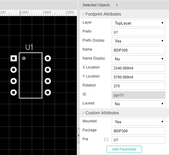
EasyEDA Schematic File Object
Note: Schematic, Schematic Symbol, Spice Symbol, Subpart and Subckt use the same format.
EasyEDA Schematic File Object is a JSON Object which allows you to hack your designs via other languages, such as Javascript, Python, PHP, C, C++. The interesting thing is that your can control/modify your design in EasyEDA editor via Javascript language.
Rules
JSON Keys
Every EasyEDA graph unit has an unique key, such as "wire", "Symbol", "junction", "bus", "busentry", "netlabel", "netflag", "pin", "polyline", "path", "arc", "rect", "polygon", "arrowhead", "ellipse", "image"
itemOrder key
Because an object in EasyEDA is an unordered set of name/value pairs in JSON format, but EasyEDA's graphs are ordered. We need an array to store the order of these objects. Every schematic lib has an itemOrder key and the whole JSON object has an itemOrder key.
Example
File
 Open Schematic Example
wire
"wire":{
    "gge48":{
        "gId":"gge48",
        "strokeColor":"#008800",
        "strokeWidth":"1",
        "strokeStyle":0,
        "fillColor":"none",
        "pointArr":[
            {
                "x":290,
                "y":430
            },
            {
                "x":370,
                "y":430
            },
            {
                "x":370,
                "y":490
            }
        ]
    }
    ..........
}
All wires will be stored to wire key, their id will be taken as the key such as gge48.
Symbol
All schematic components will be stored to Symbol, their id will be taken as the key such as gge7. Schematic component JSON is a little bit complicated, it has lots of other JSON Keys, such as polyline, image, path etc.
Note: please check the other shapes format via below JSON example
JSON example
check the complete JSON object via github gist Schematic Json object
EasyEDA PCB File Object
Note: PCB and Package use the same format.
EasyEDA PCB File Object is a JSON Object which allows you to hack your designs via another language, such as Javascript, Python, PHP, C, C++. The interesting thing is that your can control/modify your design in EasyEDA editor via Javascript. So you can use codes to create your own outline.
Rules
JSON Keys
Every EasyEDA graph unit has an unique key, such as "TRACK", "PAD", "VIA", "TEXT", "DIMENSION", "FOOTPRINT", "ARC", "RECT", "CIRCLE", "HOLE", "COPPERAREA", "SOLIDREGION", "DRCRULE", "FABRICATION"
itemOrder key
Because of an object in EasyEDA is an unordered set of name/value pairs in JSON format, but EasyEDA's graphs are ordered. We need an array to store the order of these objects. Every package has an itemOrder key and the whole JSON object has an itemOrder key.
Example
File
 Open PCB Example
TRACK
"TRACK":{
    "gge6":{
        "gId":"gge6",
        "layerid":"1",
        "net":"S$7",
        "pointArr":[
            {
                "x":357,
                "y":171
            },
            {
                "x":456,
                "y":171
            }
        ],
        "strokeWidth":1
    }
    ......
},
All tracks will be stored to TRACK key, their id will be taken as the key such as gge6.
SIGNALS
EasyEDA groups all of the objects with the same net name in one array.
FOOTPRINT
All packages will be stored to FOOTPRINT, their id will be taken as the key such as gge7. PCB package JSON is little bit complicated, it has lots of other JSON Keys, such as TRACK, ARC, RECT etc.
Note: please check the other shapes format via below JSON example.
JSON example
Check the complete JSON object via github gist PCB Json object