EasyEDA Std Schematic FAQ
Schematic
If I update the schematic, how do I then update the PCB?
Using: "Menu - Design - Update PCB".
Alternatively, you can import changes from the schematic from within the PCB Editor:
https://docs.easyeda.com/en/PCB/Import-Changes/index.html
How to rename a Sheet/Page or modify description.
In this menu, there is a Modify option, so you can rename your files. Double click or right-click the sheet tab can change the sheet title too. 
What is the unit of the schematic sheet? How to change schematic unit?
The basic unit of the schematic sheet is the pixel. 1 pixel is about 10mil (0.001 inch) but please note that this use of the pixels as a unit in a schematic is just for reference.
For a complex project, I want to split the schematic over several sheets. Does EasyEDA support hierarchy?
EasyEDA don't support hierarchy, but support multi-sheets。 Please check out this link https://docs.easyeda.com/en/Schematic/Multi-Sheet/index.html
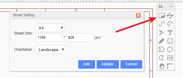
How to change the sheet size and modify the design information.
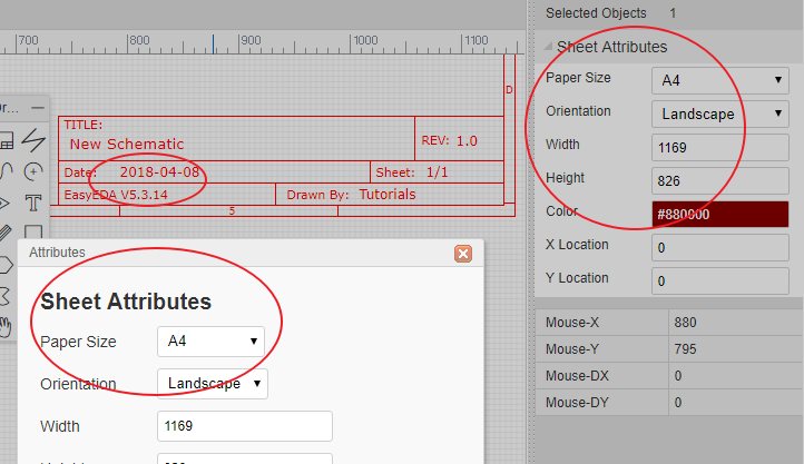
To change the sheet size, move the mouse anywhere over the lower right area of the drawing border or frame until the whole border highlights red and then right-click on it. Paper size and orientation can then be changed in Sheet Attributes in the right hand panel.
To modify the design information, left-click on the relevant blue text in the lower right area of the drawing border or frame to change it in Text Attributes in the right hand panel. Double left-clicking the blue text will allow you to type new information directly into the field.
How to indicate low electronic level in the Schematic Pin or Netlabel
You can add a # characater in the pin name/netlabel last text. You can use symbols that you are familiar with. You do not have to add a line above the netlabel name.
I can't convert schematic to PCB. Why is this?
- You have not set the right footprints for your components.
- Prefix Conflict Error
- Invalid footprints
How to use the function of cloning?
Details
Click the schematic diagram or pcb that needs to be cloned, select it and click the right mouse button to select the cloning function. 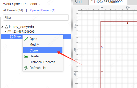
Note: The cloned schematic diagram or pcb may not have the same name. Different names must be used.This completes the cloning.There is no limit to the number of clones.PCB can also be cloned. 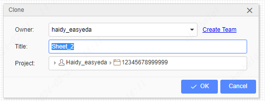
How do you change the size of the canvas grid?
Details
In the schematic screen, click on the blank space of the canvas to change the grid size of the canvas in the right property bar. 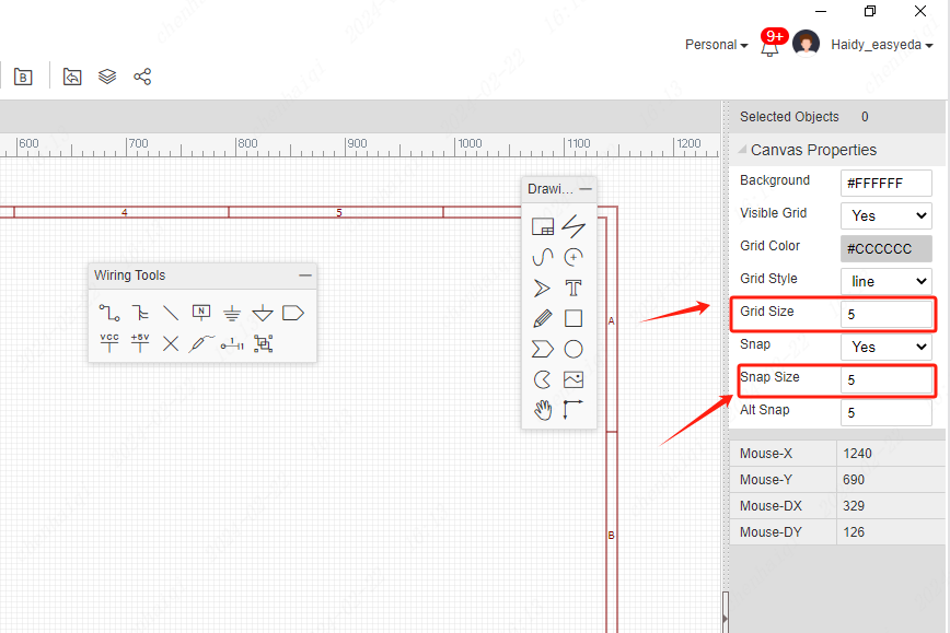
Grid Size:Represents the size of a single grid. Snap Size:Represents the distance size of the moving grid. The pcb interface is also modified in the same way. 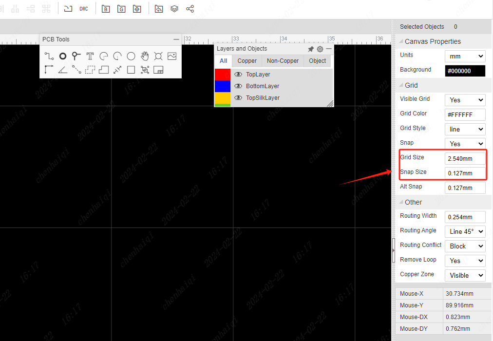
How to set schematic components not to update to pcb?
Details
Select the component in the schematic and modify the ‘Convert to PCB’ property in the right property bar. 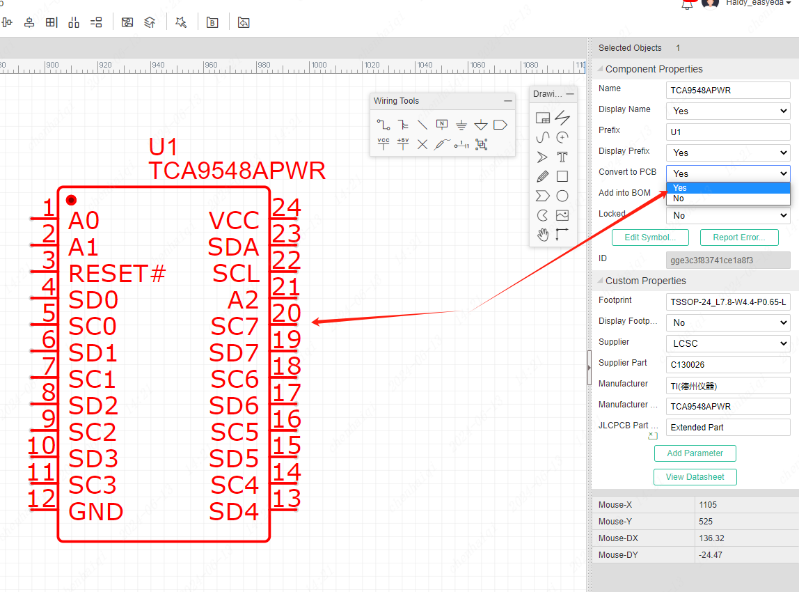
How does the schematic highlight the network?
Details
Step 1: Find the net category in the project design on the left side, then select the network you want to highlight in the schematic and click on it. The system will automatically position it on the canvas and highlight the network in red. (as shown in the figure arrow 1.2.3.4. pointed) 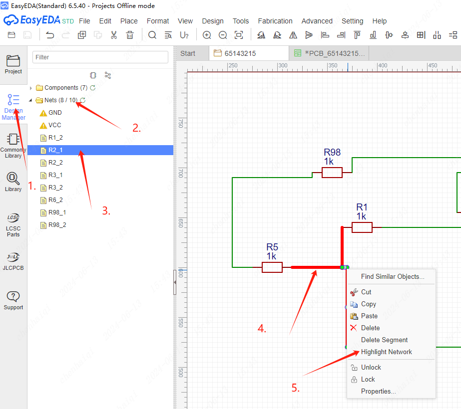
Step 2: If you want to highlight this network continuously, you can select this network, click the right mouse button, and choose "Highlight Net" in Mail Options. Step 3: If you want to cancel the highlighting also in the same way, click the right mouse button.
How to show and hide the Prefix of a device?
Details
In the schematic or in the pcb, you can select the device and then modify the properties of the ‘Display Prefix’ in the right property bar. 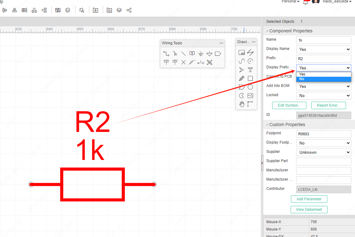
The same way in PCB. 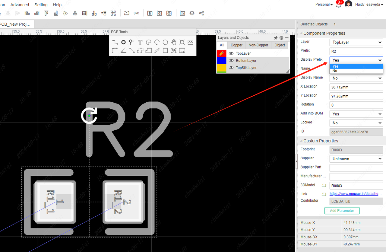
How to remove a component from the bom file?
Details
In the schematic or in the pcb, you can select the device and then modify the properties of the ‘Add into BOM’ in the right property bar. 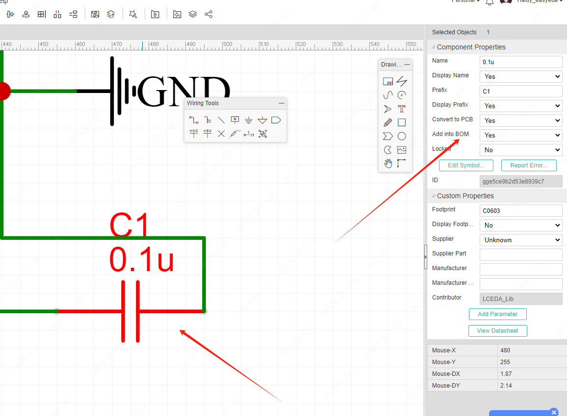
The same way in PCB. 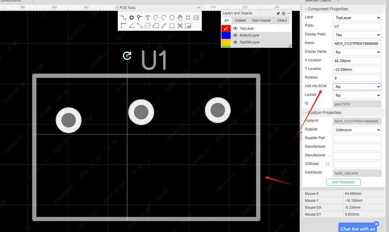
After the setup is completed, export the bom file again, and then check whether the component has been removed from the file. After confirming that there is no problem, you can export the bom file and then place an order. 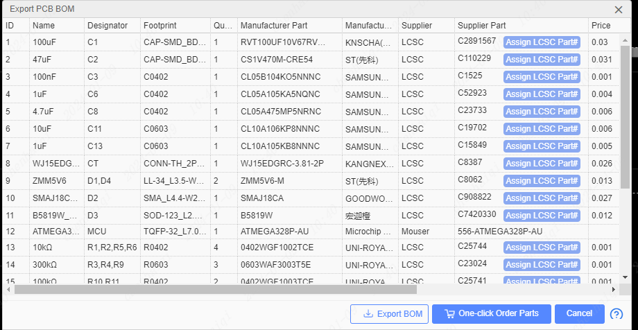
How to do copy and paste?
Details
When we want to reuse the schematic design or PCB design or move it to another project, we can use the copy-paste function. First you need to open the schematic or PCB of both projects at the same time, then copy one and paste it into the other. You can also use the shortcut keys "Ctrl + v" and "Ctrl + v" to copy and paste.
How to change the background color of the pcb and schematic in the standard version?
Details
The color of the background can be modified in the property bar on the right side of the panel. 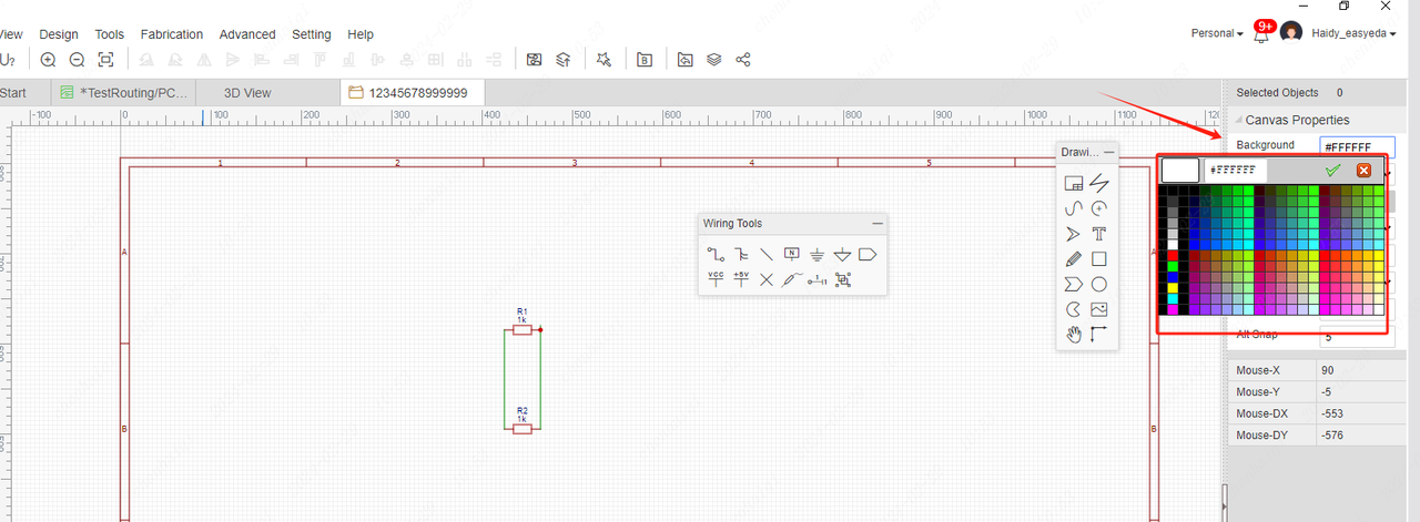
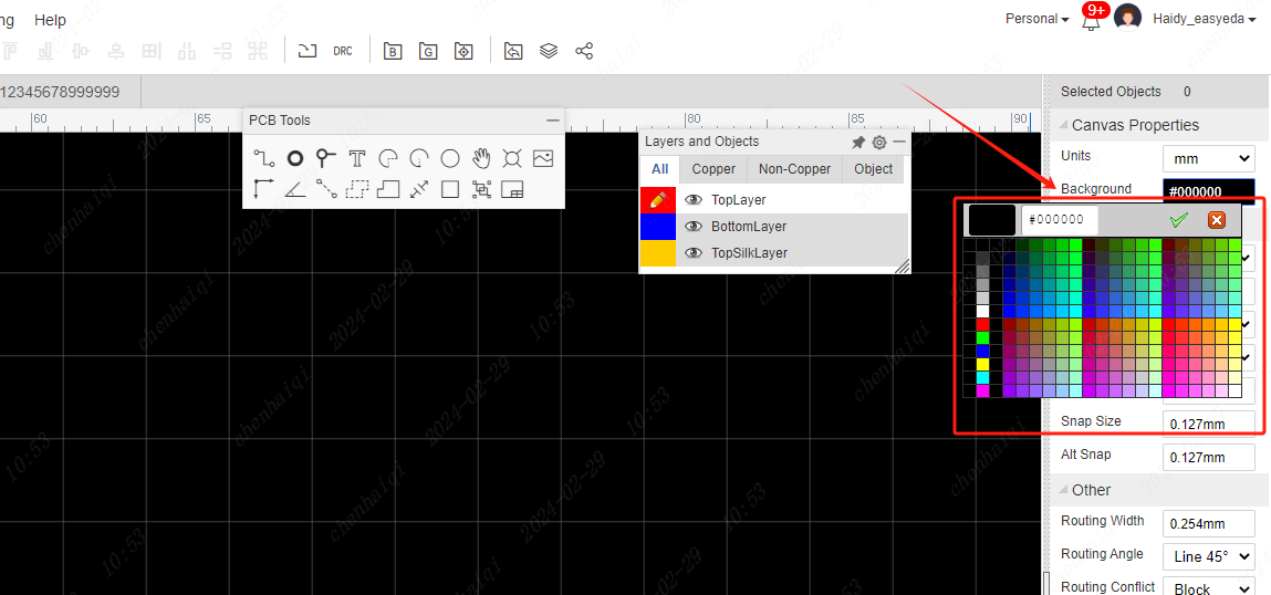
How to change the editor language?
Details
The standard version supports switching the language of the editor, which can be found inside Settings on the top menu bar. 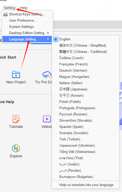
How do you fix the duplicate Prefix error?
Details
An error like the one shown below. 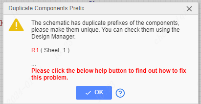
In this case, you need to find the repeated bit number in the schematic, which is "R1".Click on Components in the Design Manager on the left, here you can see all used components with their Prefix.You can find duplicate prefixes here. 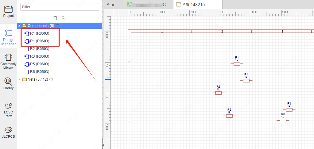
Then select the component and change it in the right property bar. 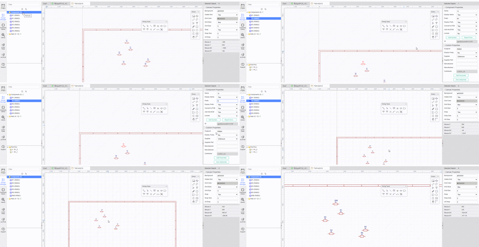
How to solve the error reported by the symbol and footprint pin mismatch?
Details
When we encounter this error, it means that the number of pads on the device's symbol pins and footprints do not match and they need to be changed to the same number. 
Step 1: Find the wrong device, select it and click footprint in the right property bar. 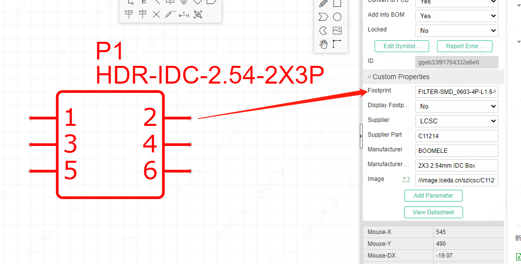
Step 2: Enter the package manager and you can see that the number of symbol pins is not consistent with the number of pads on the footprint.We can replace them with other footprints on the right side. 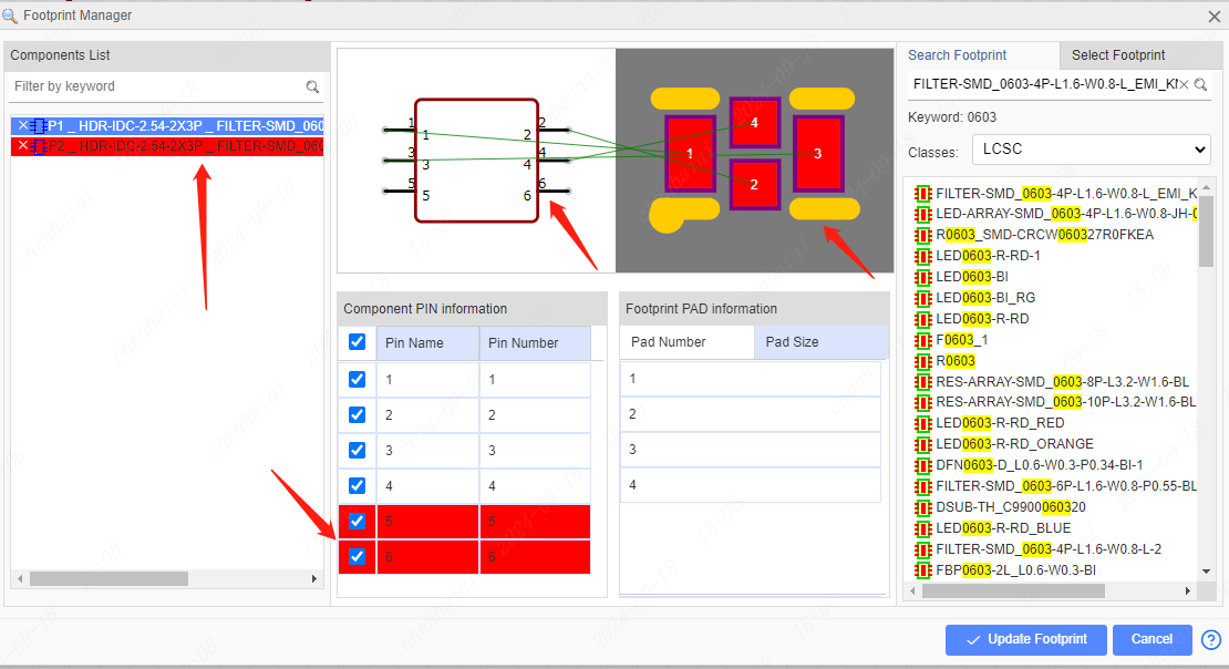
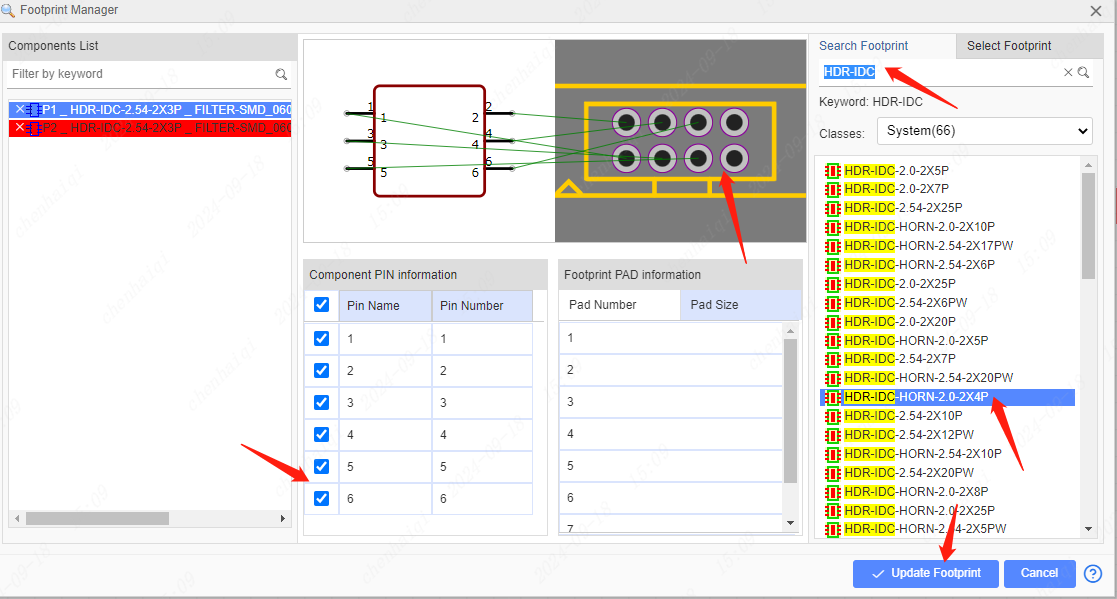
Note: The number of footprints can only be greater than or equal to the number of pins in the symbol.
How to solve the error ‘No footprint, please associate the footprint first.’?
Details
When we do a schematic update pcb, this error occurs because the symbols in the schematic are not bound to footprint, so the pcb cannot be updated.  Solution: Find the symbol in the footprint manager and check if the corresponding footprint is bound, if not, bind the footprint you want in the system library or in your personal library.
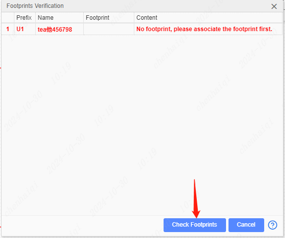
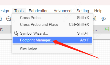
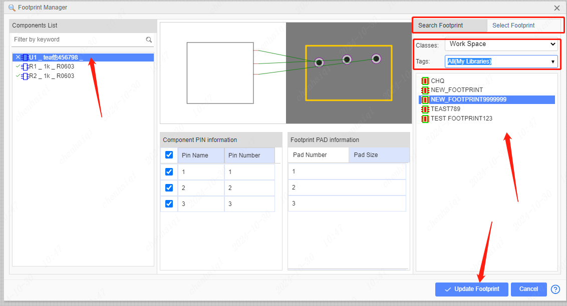 Once the update is complete you can see that the symbols have been bound to footprint, then the pcb can be updated again.
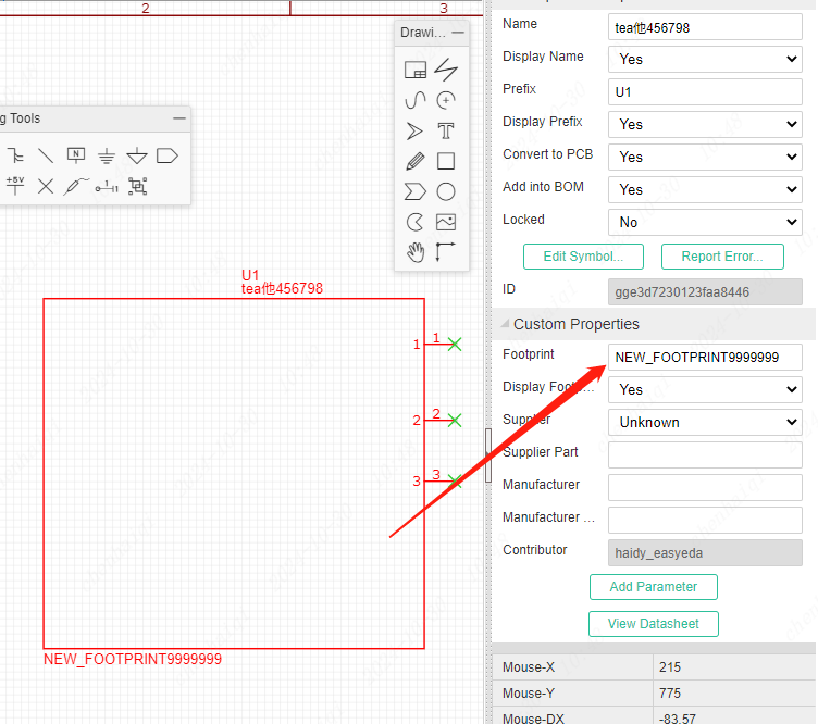
How to place the pins?
Details
In the standard version, the schematic allows direct placement of symbol pins. 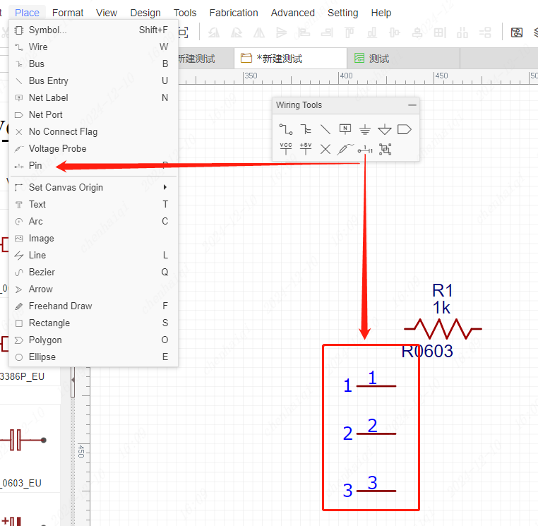
How do I fill the inside of a symbol with colour?
Details
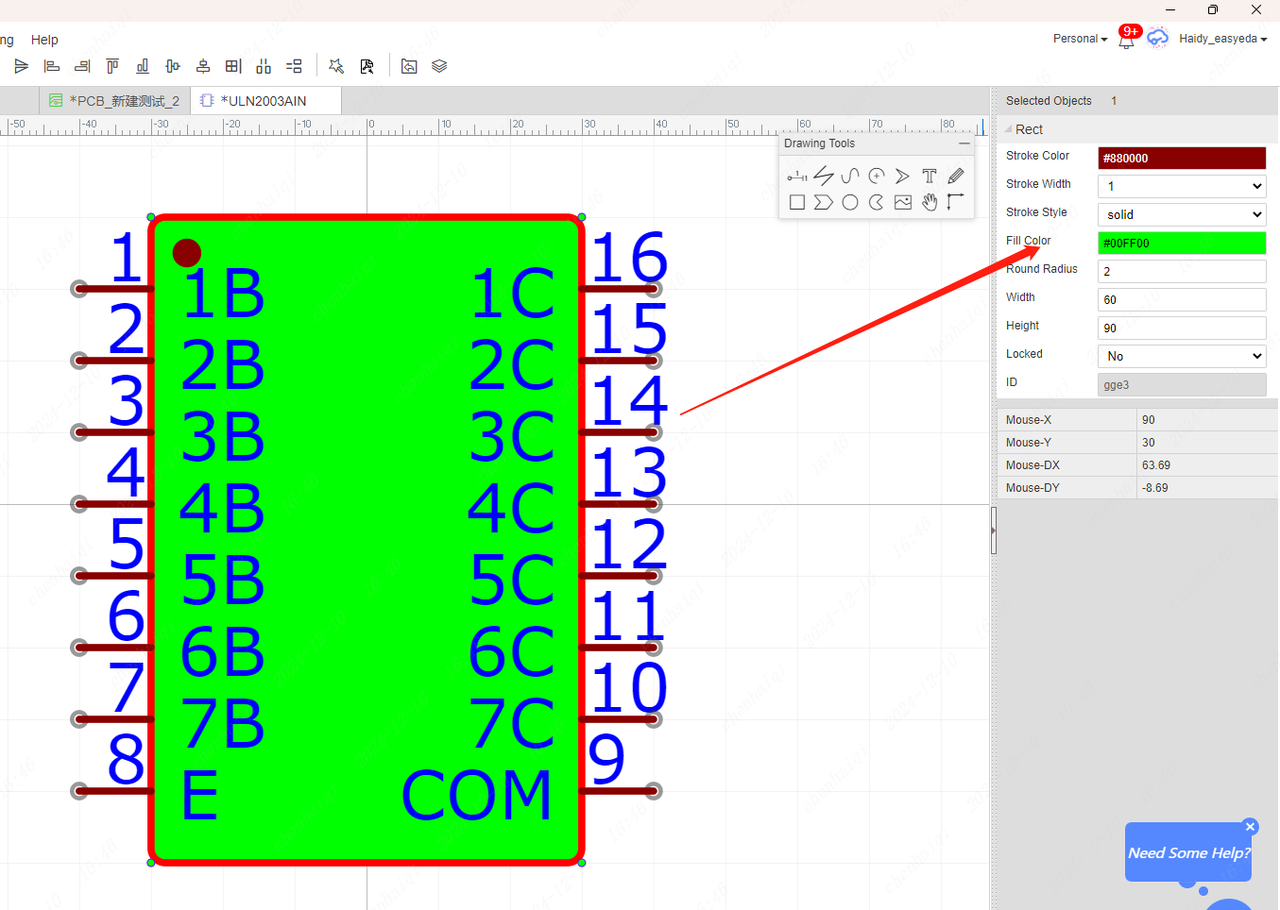
Step 1: Select the symbol you want to edit in the library and click ‘Edit’. 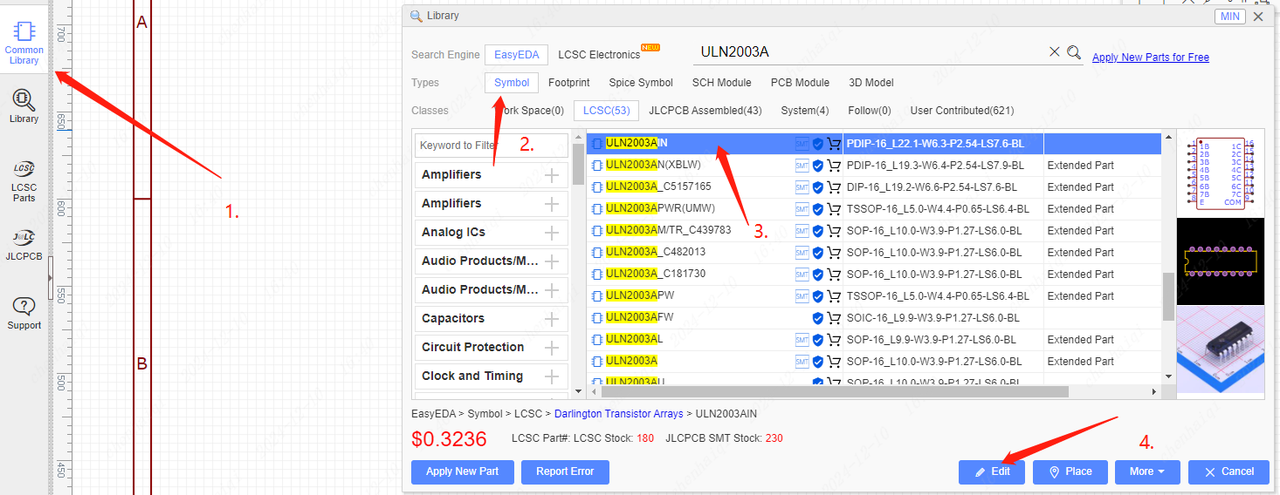 Step 2: Click on the symbol border and you will be able to choose the fill colour in the right property bar. The purpose of colour-filling symbols is to distinguish well between different designs of the same component.
How to modify the dimensions of the drawing?
Details
You can change the size of the drawing by clicking on the drawing's borders, and in the right-hand properties column you can change the size of the drawing. 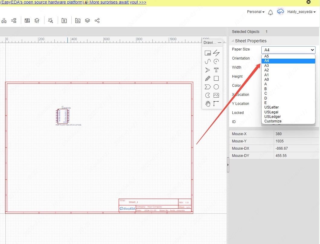
How to mirror symbols in schematic?
Details
If you want to mirror the symbols in the schematic, you can first select the symbols and then press the shortcut keys ‘X (mirror left/right), Y (mirror up/down)’.
How to create your own drawing template?
Details
Step 1: Select the drawing border in the schematic interface and right-click to select the function. 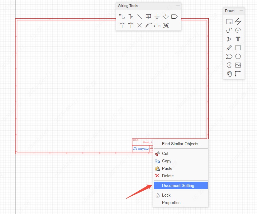
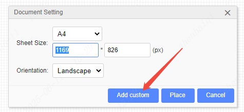
Step 2: Modify the drawing's properties and information according to your own needs. 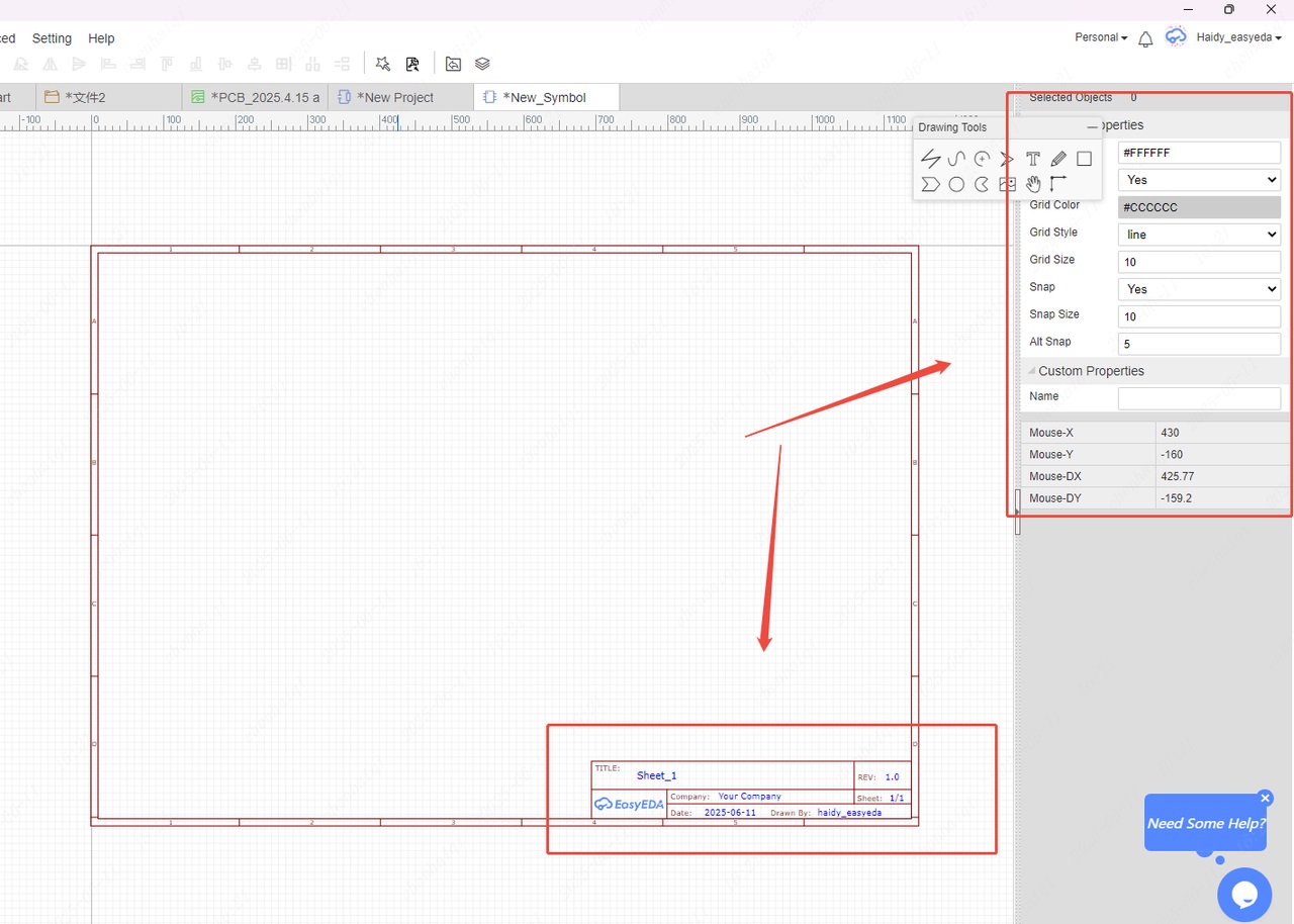
Then click Save to complete the creation, and the drawing will be saved in your personal library. 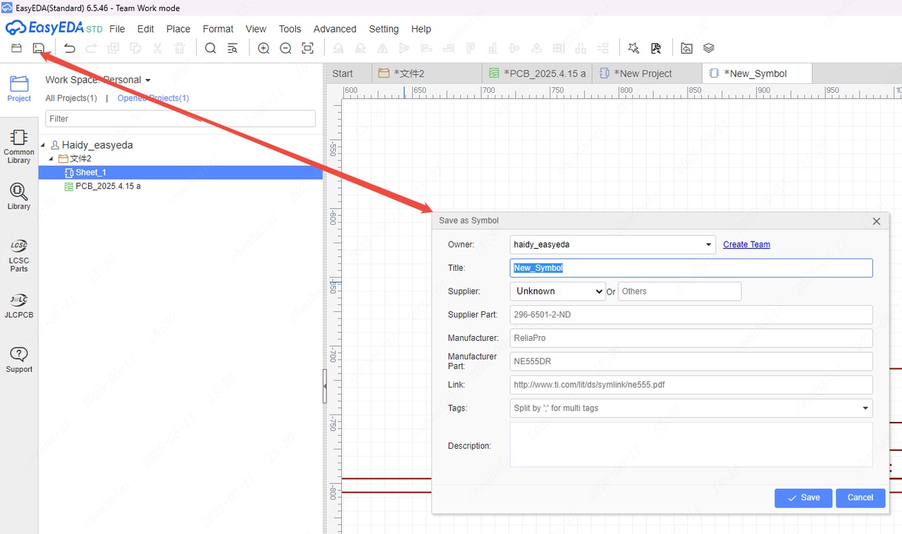
Finally: You can find this drawing template in your personal library, and then place it on your canvas like placing a symbol, and then delete the old template. 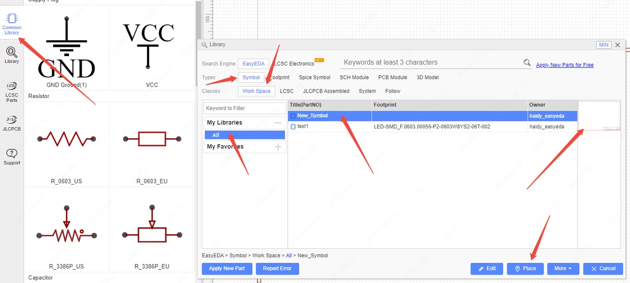
What to do if a single pin error occurs?
Details
The single-pin network error means that one of your networks is only connected to one pin. 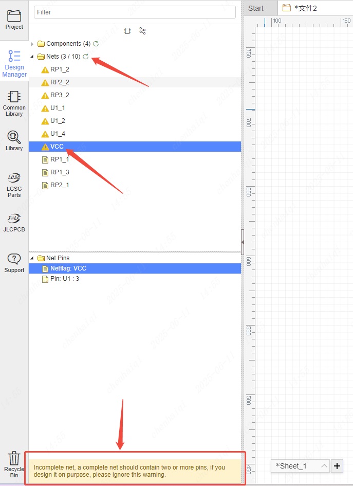
Generally, a network name needs to be connected to two or more pins to form a connection. For example, as shown in the figure below. 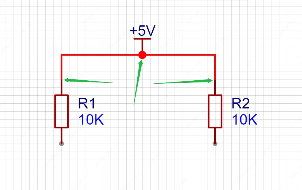
When an error occurs, it means that a network is only connected to one pin, as shown in the figure below. 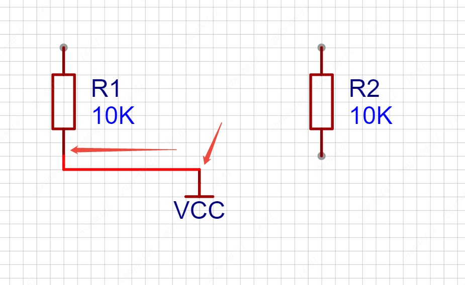
But this error is not an error that must be corrected. Because in some designs, such a single-pin design is required. It is just a reminder to tell you that you need to pay attention to this. So whether the design needs to be modified depends on the designer's own judgment. If you want to solve this error, it is very simple, just connect another pin.
How do I change the pin numbering of a symbol?
Details
Select the symbol and right-click to enter the symbol editing interface. 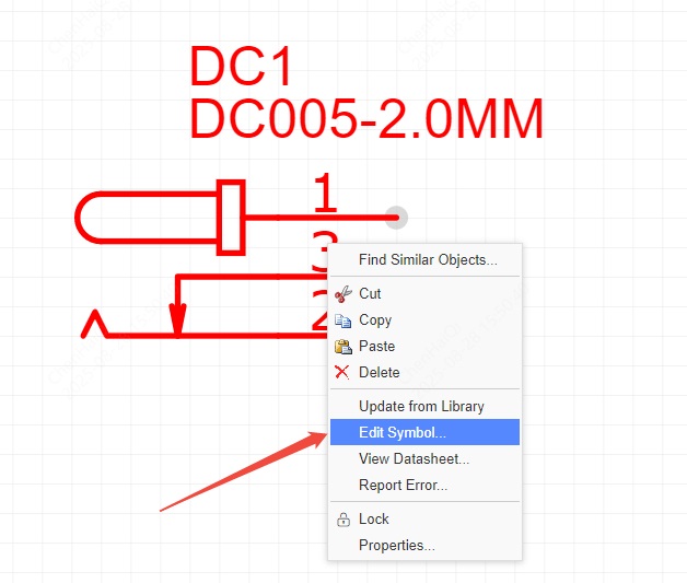
Then you can modify the pin number and pin name of the symbol. However, please note that the pin number and pin name of the symbol must be consistent with the pad number and pad name of the footprint. 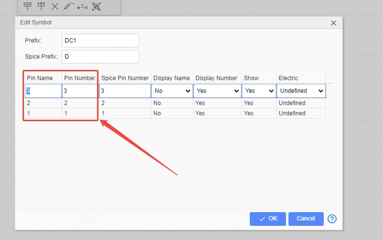
How do I set whether to retain the original reference designator after copying and pasting?
Details
In the settings at the top menu bar, check this option. If checked, when copying and pasting components or designs, the prefix of the components placed on the canvas will be automatically updated. If unchecked, it will not be updated and the original prefix will be retained. 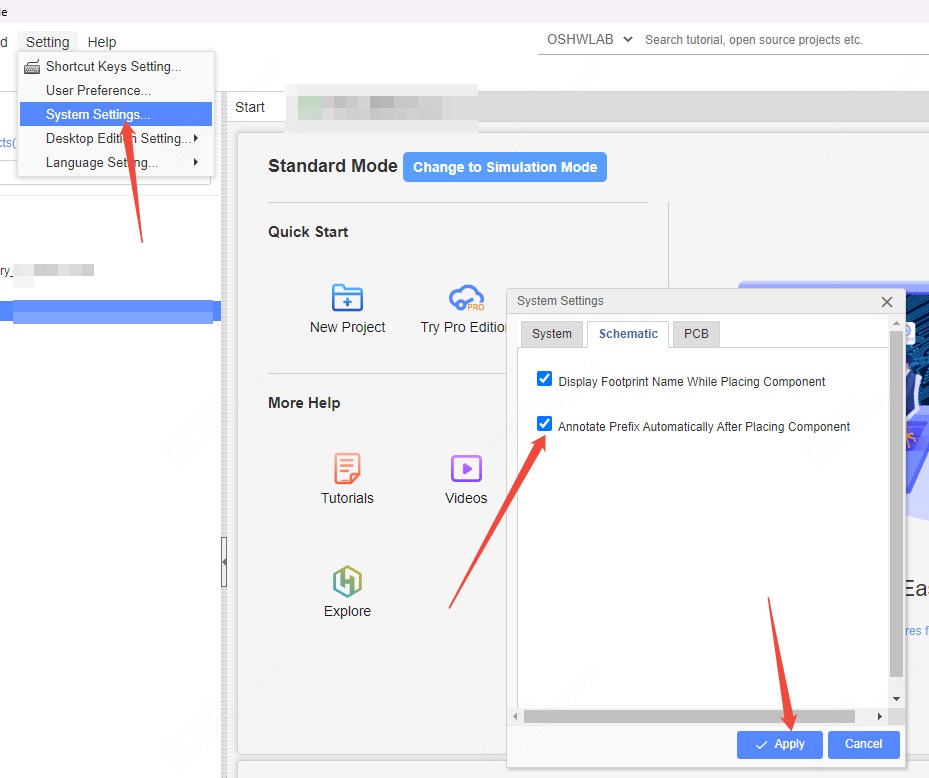
How do I export image files?
Details
Both the schematic diagram and the PCB interface can be exported as image files via the top menu bar. 

How to align the grid?
Details
Under normal circumstances, as long as the "snap" feature is enabled, the mouse will move and align according to the grid points. If you find that the mouse is not snapping to a grid point, causing elements to be out of alignment, you can use the grid alignment feature. The function of aligning the grid is available in both schematics and PCBs. 

How to place multiple components?
Details
In EDA, there are multi-component devices. A multi-component device is a device that has two or more symbols but only one footprint. Furthermore, the prefixs for multi-component device symbols in EDA is as follows: for example, (U1.1, U1.2...), (R2.1, R2.2, R2.3...). Therefore, you should also pay attention to this issue when you need to create multi-component devices or modify device prefixes. When placing components, it's important to click continuously; you can't place a component, cancel, and then re-place it. 
How can I import a DXF file into EasyEDA and use it as an element?
Details
Both schematics and PCBs can import DXF files as line elements. The function to import DXF files can be selected in the top menu bar of the schematic diagram. 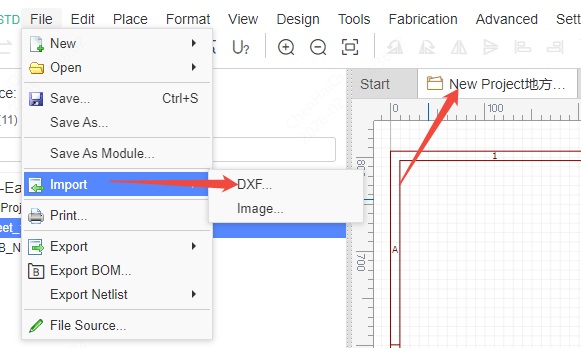
After importing, select the imported lines, and you can modify some attribute information in the properties panel on the right. 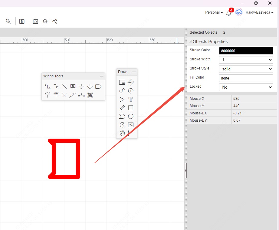
You can import files in the same way in a PCB. 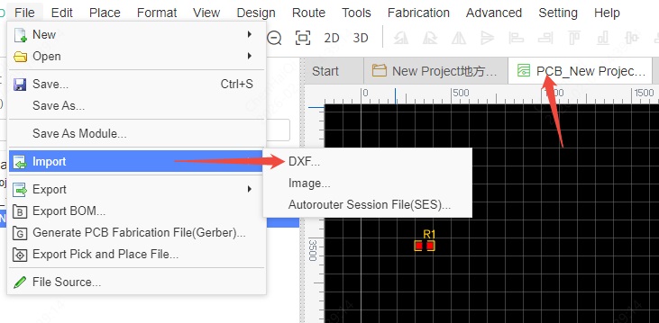
In the import interface, you can choose which layer you want to place these lines on. 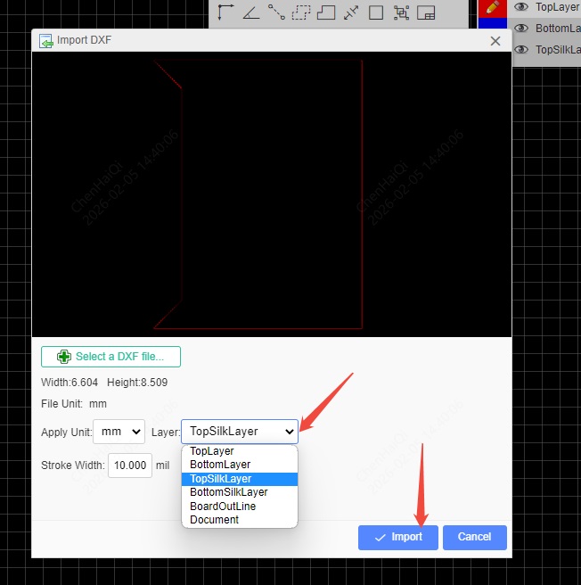
You can also select the lines after placing the DXF file and modify their layer in the properties panel on the right. Alternatively, you can select the lines, right-click, and then select "Convert to solid region". 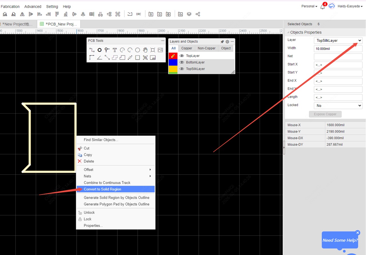
This allows you to import DXF files and transform them into board outlines, silkscreens, copper pours, and other elements. You can also place them on different layers.
How to export a custom PDF file?
Details
Both schematics and PCB layouts can be exported as PDF files, and both can be exported as custom files. In the schematic interface, you can find the export function in the top menu bar. 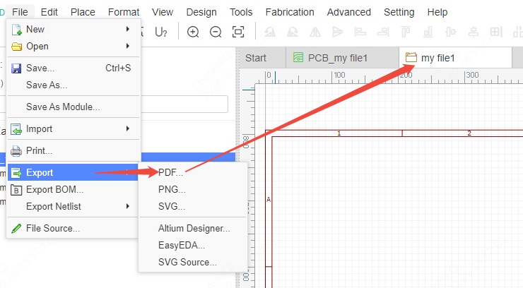
In the export panel, you can see some custom options, which you can choose according to your needs. 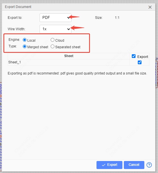
The same applies to the PCB interface. 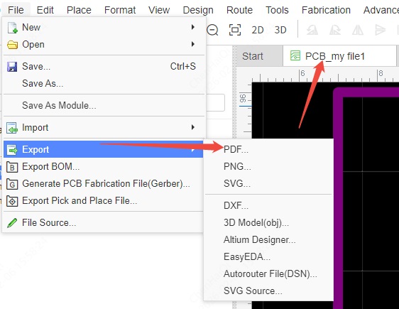
PCBs also have the same basic settings as schematic diagrams. But most importantly, the PCB supports customizing the settings for each layer. 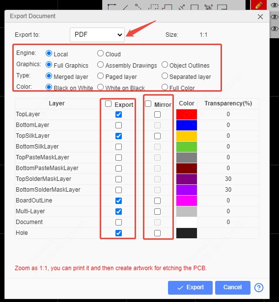
After setting all the configurations, you can export the PDF file you want.
How to show or hide device pin numbers in a schematic?
Details
Place the component symbol in the schematic, select it, and click the "edit symbol" function in the right-hand properties panel to open the editing panel. You can then set whether to hide the pin name and pin title. 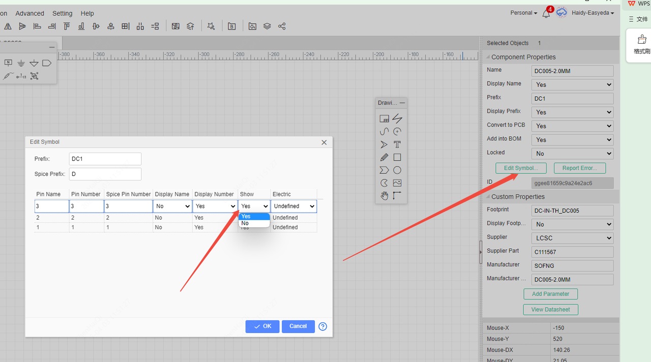
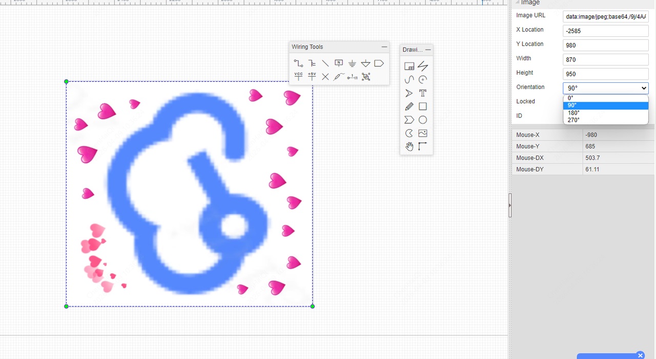
How to rotate a schematic and resize imported images?
Details
Step 1: Import the image. 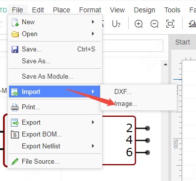
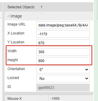
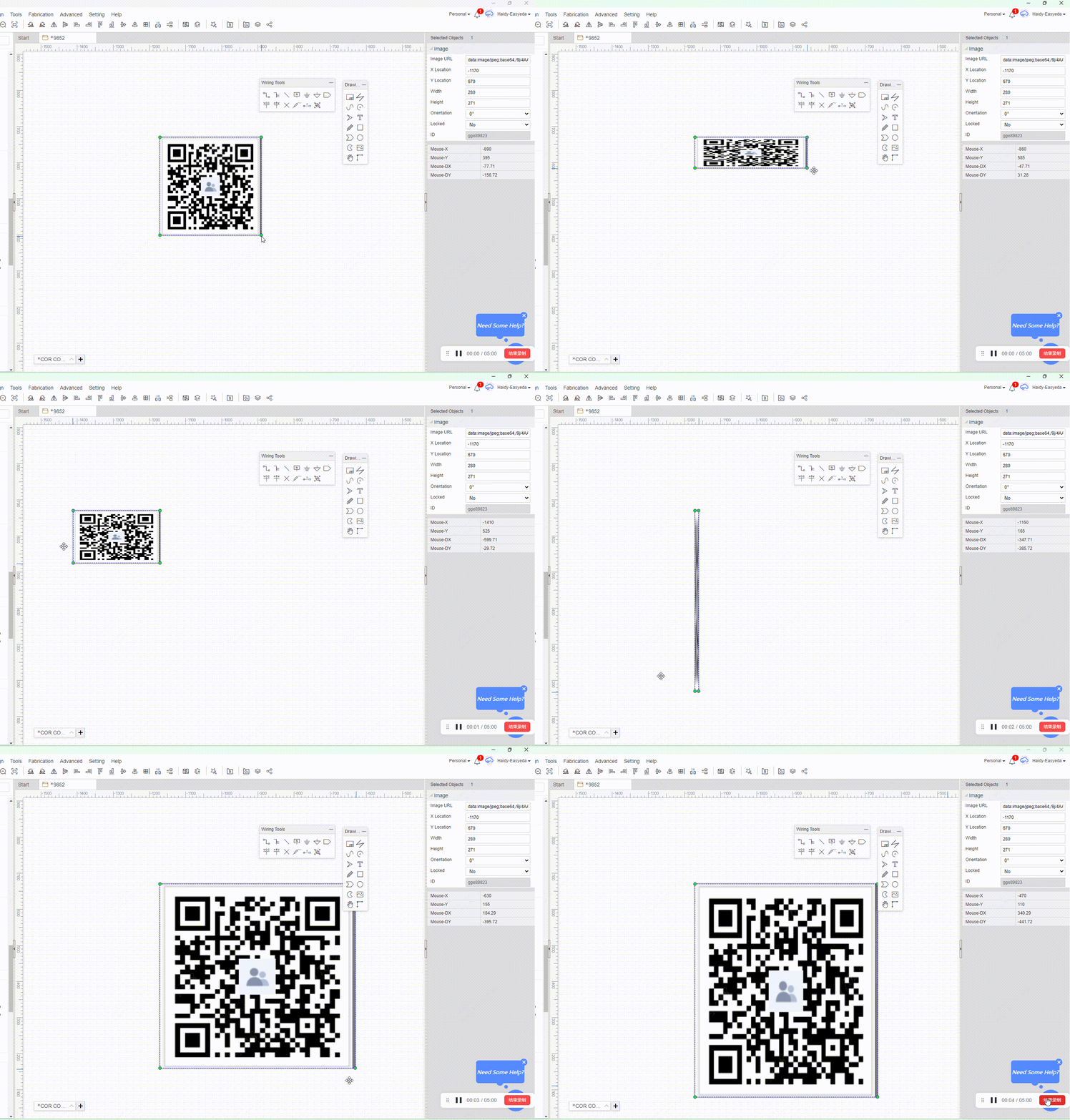
Step 2: Select the image and choose the rotation angle in the properties panel on the right.You can also modify the height and width. 