Copper Area
Copper Area
Sometimes you will want to fill in or flood an area with copper(Copper Pour). Normally after drawing the copper area, set the net it is to be connected to (floating copper areas are not recommended because they can cause EMC and Signal Integrity (SI) problems).
Before using Copper Area, please make sure your PCB has a closed board outline!
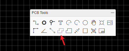
Usually this copper area will be connected to a net such as GND or a supply rail. You can draw the outline of a flood using the Copper Area button from the PCB Tools palette.
Copper Area Attributes
When selecting the copper area outline, you can find its attributes from the right hand Properties panels.
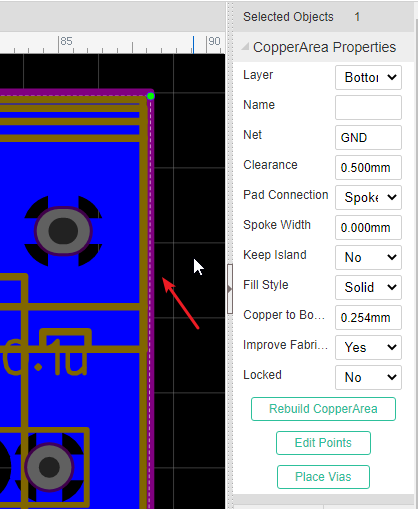
Layer: Bottom, Top, Inner1, Inner2, Inner3, Inner4 etc.;
Net: the net that the copper area is connected to;
Name: set a name for it.
Clearance: clearance of the copper area from other nets and floods;
Pad Connection: direct or spoke (i.e. a cross shaped heat shunt);
Spoke Width: When Pad Connection is Spoke, you can set the Spoke width, which is copper area fill connect with Pads.
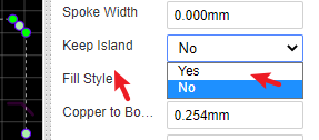
Keep Island: Yes/No. This keeps or removes any isolated areas of copper created as part of the flooding process. It is usually good practice to removes these unless you really need them to maintain a more even spread of copper (copper balance) on your PCB.
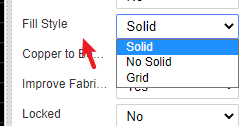
Fill Style: Solid/No Solid/Grid. Selecting No Solid will removes the fill so that you can see the tracks more clearly; when select Grid, you can set the grid spacing and grid width.
Copper to BoardOutline: Setting the clearance between copper with board outline.
Improve Fabrcation: Yes/No. If you set as No, you will see much sharp copper corners, that is not good for PCB fabrication.
Rebuild CopperArea: Click the button to Rebuild Copper Area if you make any changes.
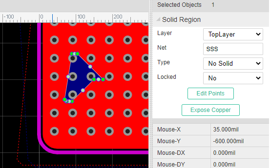
Edit Points: You can edit the copper area shape manually, any shap as you want.
Add/Remove Vias: When you add copper areas at two and more layers which are having same net, you can add multiple vias for the copper fill area, just click the "Add/Remove Via" button, then set the via parameter. The vias will avoid the objects if the via conflict the DRC. 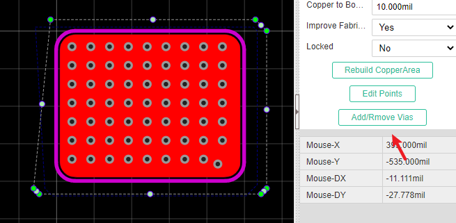
Tips
- Hotkey
Eto start draw copper area. - Hotkey
Lto change drawing type(90 degrees or 45 degrees or Arc) - Hotkey
Shift+Bto build all of the copper areas. - Hotkey
Shift+Mto hide copper areas fill zone, just show the copper outline. - Hotkey
DeleteorBackSpaceto redo previous steps. - If you after copper pours but no copper fills show up, you need to set it a net same one of the PCB nets, or keep the island as YES, and the rebuild the copper area via "Rebuild Copper Area" button or "SHIFT+B".
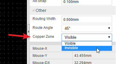
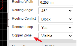
- If you want to hide the copper area and keep routing tracks, you can set the copper zone invisible at the right-hand panel.
- If you want to cutout some copper corners, you can use "Solid Region - No Solid", and then set different net for it, and rebuild the copper area.
Notice
Because of the browser's performance issue, EasyEDA doesn't support the real-time copper pour, after PCB modifying, please rebuild copper area via Hotkey
Shift+B.EasyEDA doesn't support click the copper zone, you need to click the copper outline to select it.
If the PCB size is more than 15MB, the copper filled data is stored in the client or browser(that is because some copper filled data is too large to save at server), and the copper area outline data is stored in the file. Therefore, when the PCB is opened for the first time, the copper area filled data will be automatically pouring and saving at local, and the second time the PCB is opened, the filled data will be automatically loaded from the local storage. When you need to draw the forbidden copper-laying area, please use the "No Solid" property of "Fill Type" to cutout the copper area and rebuild it, do not use the operation of drawing the area with wires or circles and then removing the wires or circles to create the forbidden copper pour area. If the PCB size is less than 15MB, the copper filled data will be saved into file, and you can open the PCB in another PC without rebuild copper area.
FAQ
Why sometimes it takes a long time to copper pour
Check that the PCB has a large number of polygon pads, which generally appear in the PCB imported Altium Design files, and if so, manually modify them to Round or Rectangle pads.
Check if there are a large number of wire arcs, generally appear in the imported Altium Design PCB, Altium Design picture is a large number of track segments combined, need to be manually removed.
Check that the board outline is complicated, with overlapping board outlines, or a large number of board outlines, adjust them manually to reduce the number of board outlines.
Why did I not show the copper fill after copper poured
Your copper area net must have the same pad or via same as the current layer, otherwise it will be considered an island to be removed. Click on the copper wire frame to modify the net in the property panel on the right. For example, your pad net is
VCC, you lay copper net needs to be set toVCC.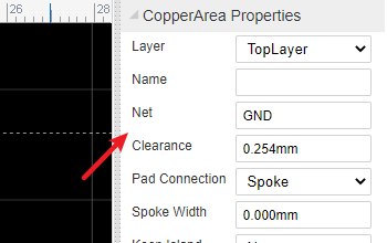
If you don't change the copper area ne, you can click on the copper outline and modify the property "Keep Island" to Yes in the right property panel. The copper area logic of the EasyEAD is based on whether there is a connection or not to decide whether it is an island, and if there is no element connection to the same net, the copper area will be considered an island.
Check that the editor version is 6.3 above, 6.3 PCB board open in version 6.2 can not properly copper pour. Please CTRL+F5 refresh editor page upgrade to 6.3, if it is true that can not upgrade to 6.3, you must remove the copper area and redraw.
Check that the board outline is closed and that endpoints need to be closed between the tracks, and that there are overlapping segments of the board outline (usually inside the imported PCB). Once you can hide all layers, only the board outline layer view is displayed, and each segment is carefully examined.

Check that the copper area property is set to type No Solid and needs to be set to Solid or Grid.
Whether to make the copper area invisible, on the right side of the canvas, set the copper zone to Visible.
Still unable to copper pour may be an editor bug, please contact us.
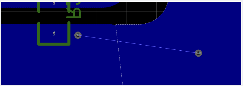
Why the ratline doesn't disappear when two copper area overlap which are the same net
- At present, doesn't support this, that will make the ratline generation very slow. Please route a track manually to connect these copper areas.
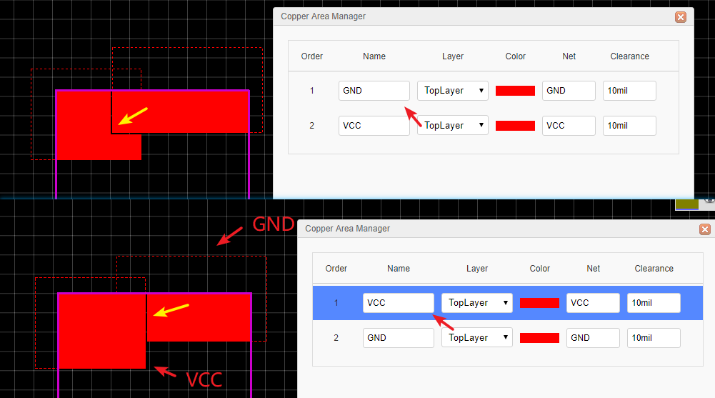
Copper Area Manager
EasyEDA support copper area manager now, you can set the copper order and apply, the forward copper area will be poured first.
Via: Top Menu - Tools - Copper Area Manager
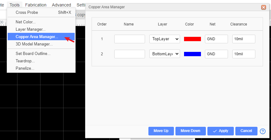
For example: The GND on the top and VCC on the top, you can see the clearance is different.