Route Tracks
Route Tracks
In the schematic editor, we use Wire or the W Hotkey to connect Pins, in a similar way in the PCB editor, we use Track to connect Pads. Track allows you to draw PCB tracks and can be found on the PCB Tools palette or using the W Hotkey (not T).
Some Tips about Track
Single click to start drawing a track. Single click again to pin the track to the canvas and continue on from that point. Right click to end a track. Double right-click to exit track mode.

Drawing a track at the same time as using a hotkey(for example hotkey
B) for changing the active layer will automatically insert a Via:
If you start drawing a track on the top layer, you will see it drawn in red, then press the B key to change to bottom layer and you will see EasyEDA insert a grey via and then the track will continue being drawn but now on the bottom layer in blue.
Pressing the
+or-Hotkeys when drawing the track will change the width of the track on the fly. Use the hotkeyTABto change the track width.
Double clicking on a drawn section of the track will add a new vertex at that point. You can drag the vertex to form a new corner. And you can right-click the point and delete it.

Click to select the track and then Click and Drag on a segment of the track to adjust the segment between vertices.

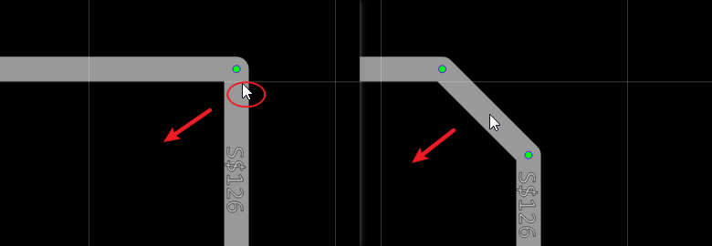
When the track's corner is a right Angle and the routing corner is 45, drag the track next to the right Angle node to make a bevel. Instead of dragging a node directly, dragging a node directly will drag the entire track.
Selected a track, you can delete its node point.

Pressing the
LHotkey when drawing the track will change the track's Route Angle on the fly. And you can change Route Angle on the Canvas Attributes of the right panel before the next drawing.
You can change inflection direction when routing, just press
Spacekey.
If you want to route a track and use "L", and the then press "+", you will get two different size track segment. or press "SHIFT+W".

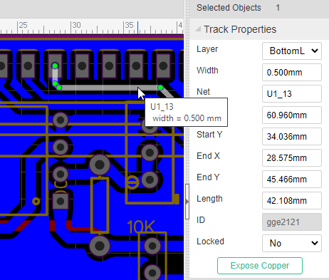
If you want to create the solder mask aperture for the track, you can use "Expose Copper" when you select the track on the right-hand panel. The solder mask will bigger 4mil than the track.

And if you want to create the slot hole, you can route a track, and then right-click the "Convert to Board Cutout" menu.

You can make track routing width follow design rule, after enable the design rule option.

Right-click the track, you can select the track connection or a whole same net tracks.

If you want to the whole track, you can press
SHIFTand move it.You can disable the DRC boundary at Desgin Rule. The size follow the rule.

If you want to continue routing for a net, you can disable the "Terminate Routing Automatically" option at "Setting - System Setting - PCB".

Set up Remove Loop while routing, it only works on copper layer.

Using Routing Conflict as "RoundTrack" will help you finish routing quickly.

When edit the footprint document, you can set up the "Cut Silkscreen" to avoid the silkscreen track overlap the pad.

Track Length
When a track is selected, you can find its Length attribute in the right panel.
At left-hand Design Manager, click a net, will pop up a dialog to show you this net track length.
Click a track, press hotkey H will keep hightlight this track and net, and show this net's length.
Delete a Segment from a Track
While routing, if you want to undo previous track path, you can press key "Delete" or "Backspace".
Move your mouse to the segment which you want to delete, click it, then hold
SHIFTand double click it. the segment will be removed. Or right-click delete the node.Right-click the track node to delete the track
Click the track, right-click delete it, or press "Delete" key directly.
DRC outline
When you routing a track on the signal layer, you will see an outline around the first track, it is the DRC outline, the clearance from outline to the track edge depends on your Design Rule(DRC) clearance setting.

Routing Conflict
When the PCB comes from the schematic converted, the "Routing Conflict - Block" will be opened automatically.
At the right-hand attributes panel - others, you can find a "Routing Conflict" option:
- Ignore: You can route the track overlap the different net name objects.
- Block: If the track net name different with other objects, this track will be blocked when routing.
- RoundTrack: The track while routing will walk arroud the different net objects.
- Push: Doesn't develop yet.
Differential Pair Routing
EasyEDA provide a easy experience for the differential pair routing. Via: Top Menu - Route - Differential Pair Routing
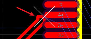
You must make sure the Differential Pair net names must be XXX_N, XXX_P or XXX+,XXX-.
and you need to set Differential Pair net rule at the "Top Menu - Tool - Design Rule" first.
How to route Differential Pair:
1.Set the Differential Pair net name as
XXX_N, XXX_PorXXX+,XXX-, and set the rule for the Differential Pair net at the "Design Rule"2.Click the menu
Top Menu - Route - Differential Pair Routing3.Click the one pad of the Differential Pair pads
4.Routing
Notice:
- Only for 45 degrees routing, doesn't support hotkey L and Space key.
- Doesn't support the fanout routing.
- Doesn't support the DRC blocking.
Known Issue:
- When finish previous routing location too close with the finish pads, the track will generate the extra segments, please finish the previous location far away from finish pads.
Track length Tunning
You can tunning your track very easy on the editor.
Via: Top Menu - Route - Track length Tuning 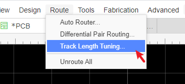
How to use:
1.Select the track which is you want to tune
2.Click the menu:
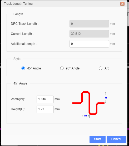
Top Menu - Route - Track length Tunning3.Set the parameter, start
4.Left-Click the track where is you want to start, and then move the mouse
5.When the track length close your setting, it will stop tunning.

Notice:
- Doesn't support one side tunning for a track yet
- Doesn't support auto push or avoid the nearby tracks yet
Cloud Auto Router
For some simple or prototype PCBs, you may want to use the auto router function to save time. Layout is a time costly and dull job. EasyEDA spends lots of time to provide such a feature and it is loved by our users. Before using the auto router, you need to set the board outline for the PCB.
Auto router is not good enough! Suggest routing manually! You can use "RoundTrack(Walk Arroud)" option to route tracks, via right-hand panel - Routing Conflict.
Steps:
1 Click the the auto router button from the Top Menu"Top Menu> Route > Auto Router"
2 Config the auto router
After you click that button, you will get a config dialog like in the image below.

In the config dialog, you can set some rules to make the auto router result professional. These rule must equalize or more than DRC setting.
General Options
- Unit: The unit follows PCB canvas unit.
- Track width: The auto-route track width.
- Clearance: The clearance of the objects.
- Via Diameter/Via Drill Diameter: The via placing by auto-router.
- Realtime Display: when you select it , the real time routing status will show on.
- Router Server:
- Cloud: Using EasyEDA online server.
- Local: Using the local auto router server, when you click the Auto Router icon, the editor will check the local router server available or not automatically. How to use please see as below.
- Router Layers: If you want to route inner layer, you have to enable the inner layer first.
- Special Nets: For the power supply track, you may want it to be bigger, so you can add some special rules.
- Skip Nets: If you like to keep the a net with no route, you can skip it. For example, if you want to use copper area to connect
GNDnet, you can skip theGNDnet. If you want to reserve the routed track, you need to select theSkip Routed Nets.
3 Run it
After click the "Run" button , The real time check box will let you see how it is going, but it will make the process a little bit slow. 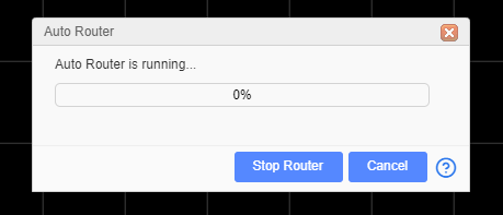
Waiting for a few minutes, after adding bottom and top copper area, you will get a finished PCB board.
When finish, will pop up a window.
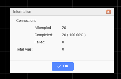
The connection means the track connect times.
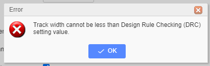
Notice:
- The parameter can't less than DRC rule, otherwise will report error.
Local Auto Router
EasyEDA suggest that using local auto router rather than using the cloud server, because when many users using cloud server, the cloud auto router will fail. Only support 64bit system.
For the local auto router, please follow the steps as below:
- 1.Download the local auto router server.
Download EasyEDA Router: easyeda-router-windows-x64-v0.8.11.zipeasyeda-router-linux-x64-v0.8.11.zipeasyeda-router-mac-x64-v0.8.11.zip
Supported OS:
- Windows7(x64) or later 64bit Windows
- Ubuntu17.04(x64) or other 64bit Linux, Linux recommend [Deepin](https://www.deepin.org)
- macOS(x64)
2.Unzip it to the User folder, such as driver D.
3.Configure the browser.Notice: Please use the latest Chrome or Firefox !!!
-   **1)Chrome**
    The Chrome Browser don't need to be configure, If the local auto router is unavailable, you have to upgrade Chrome to version 60.0.3112.78 or later. - **2)Firefox**
     1.Type "about:config" into the address bar then press enter.
     2.Search and double click the options as below (change the values to "true"):
    `network.websocket.allowInsecureFromHTTPS`
    `security.mixed_content.block_active_content`
3.Re-open Firefox.
4.Open the decompress folder, Start local Auto Router(don't need to install, just run it and keep the command window open):
- Double click
win64.batin Windows. - Run
sh lin64.shon command terminal in Linux. Open the terminal, use thecdcommand to change the directory to thelin64.shlocation, and typesh lin64.sh, then enter. - Run
sh mac64.shon command prompt in MacOS. Open the terminal, use thecdcommand to change the directory to themac64.shlocation, and typesh mac64.sh, then enter.
- Double click
5.Open the editor, open the PCB, Click the Auto Router icon at editor to start auto-router. If the local router server is available, the dialog will tell you. Click the Run button, the dialog will show the process.
Tips
Auto router is not good enough, suggest routing manually, recommed "Routing Confilct - RoundTrack" at the PCB right-hand panel. Sometimes, if you can't get it done, try the tips below.
- Use local auto router rather than cloud server.
- Make sure the net of PCB doesn't contain the special charaters, such as ` { } ^ ; ~ \ / [ ] = etc. the chrarter - and _ are supported.
- Make sure the board oultine is closed, doesn't has board oultine overlap situation.
- Make sure there are no DRC cleance errors (short circuit issue), such as two different network pads overlapping, or different net pads in the same location within the package.
- Make sure no footprint outside the board outline.
- Make sure your canvas Gird size is set to 10mil, make sure the components align with the grid via: top menu - format - align grid.
- Place some vias at suitable position, and modify the vias' net as you want.
- Make sure PCB rule doesn't have 3 decimal places, EasyEDA auto router only support 2 decimal places.
- Skip the GND nets, add copper area to GND net.
- Use small tracks and small clearance, but make sure the value is more than 6mil.
- Route some key tracks manually before auto routing and ignore them when auto routing.
- Add more layers, 4 layers or 6 layers. but that will make more cost.
- Change the components layout, make them have more space between each other.
- Don't make any via/pad overlap the different objects which can be set the net.
- Stop the auto-router, close the script, and re-open the script to run local auto-router server again.
- Sometimes, The auto-router won't work at the first time, please modify the layout and try serveral times.
- If only a few remaining networks cannot be completed, it is a normal phenomenon. Please manually route the remaining networks.
- Tell the error detail to us and send your PCB file as EasyEDA Source file to support@easyeda.com. https://docs.easyeda.com/en/Export/Export-EasyEDA-Source-File/index.html via email.
Some professional people don't like the auto router, because they think auto router is not professional, but you can use the auto router to check your placement to check the density of your PCB.
At present, the auto router is not good enough, suggest routing manually, we will improve it in the future.
Using 3rd party autorouting tools
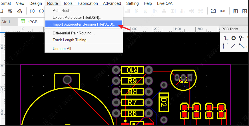
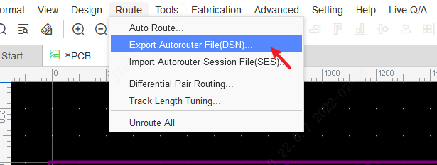
EasyEDA supports exporting auto-routing files dsn and importing auto-routing session files ses. You can use third-party auto-routing tools for wiring by exporting auto-routing files, and then import the ses files.
Steps:
1.Open the PCB to export the automatic routing file dsn, it is recommended to remove the unnecessary vias and wires first.
Via: Top Menu - Route - Export Autoroute File (DSN), or Top Menu - File - Export - Autoroute File (DSN)
2.Open the third-party auto-routing tool and open the auto-routing file DSN
Third-party auto-routing tools include: Freerouting, ELECTRA, TopoR, etc.
Freerouting download address: https://freerouting.mihosoft.eu/
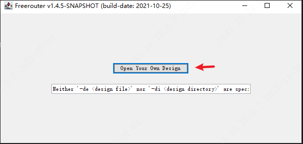
Take Freerouting as an example:
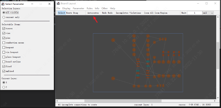
- Open Freerouting, open the autorouting file
- Set the automatic routing rules, if you do not need to set, you can directly point the routing
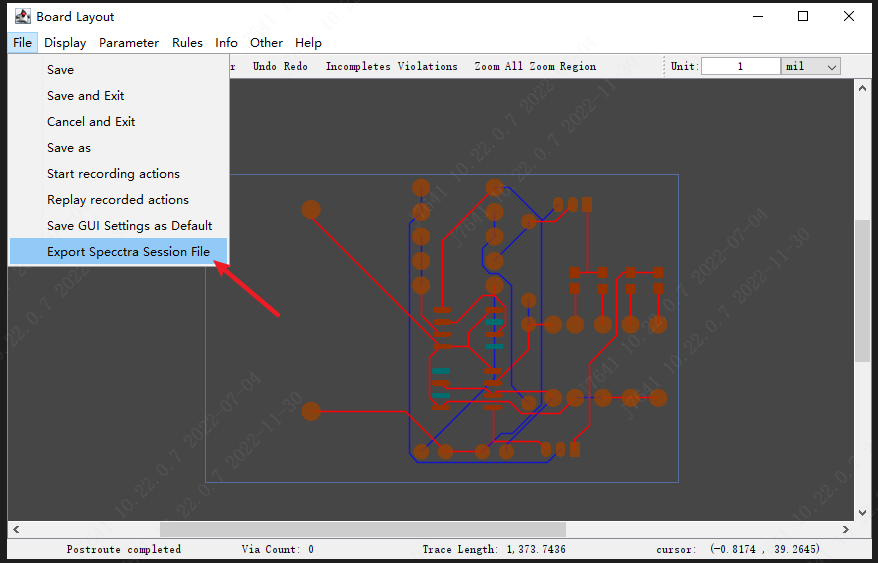
- After completion, export the automatic routing session file ses, which will be saved in the same directory as dsn
3.Import the auto-routing session file into the PCB and complete the import
Entry: Top Menu - Routing - Import Autorouting Session File (SES), or Top Menu - File - Import - Autorouting Session File (SES).