Import Altium Designer
Precautions
When you choose to import into Altium Designer, be sure to confirm the contents of the imported file.
1. The current import function is a beta version, please check carefully after importing! EasyEDA cannot guarantee a 100% match after importing!
2. Certain details may not be supported, such as design rules and internal electrical layers.
3. After the inner electrical layer is imported, the wires need to be carefully checked. The inner electrical layer cannot maintain the original network and must be reset!
The circuit design files currently supported by EasyEDA are:
- Schematic/PCB in Altium Designer/Protel DXP ASCII format
- Eagle schematic/PCB/library files
- KiCAD schematic/PCB/library files
Import steps
You can open the import dialog at File > Open.
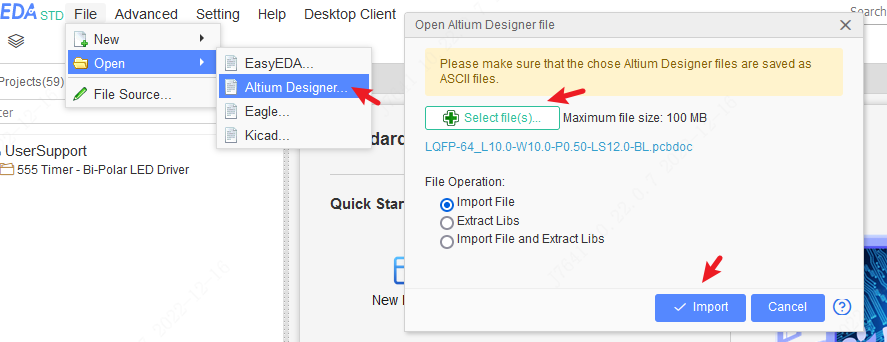
Select the Altium file, which must be a schematic file and PCB file saved in ASCII format. Please see the following tutorial for specific operations.
Choose to import files or extract libraries according to your needs.
If both the schematic diagram and PCB of the same project need to be imported, please import the PCB first and choose to extract the footprint, and then import the PCB and schematic diagram. When importing the schematic diagram, it will be automatically associated according to the previously extracted footprint title. Some footprint titles will be converted to underscores due to unrecognizable character encoding.
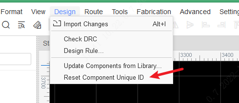
If after importing, there is no corresponding update from the schematic diagram to the PCB component, you can reset the component ID in the Design menu - reset the unique ID of the component, which is required for both the schematic diagram and the PCB. At this point, the correction of the corresponding relationship between the components on both sides is completed.
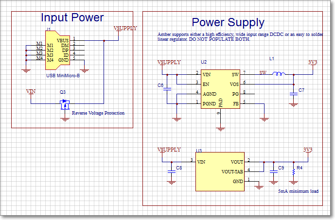
Import the schematic file of Altium Designer, the effect of the PCB file is already very good, as shown below:
Generate ASCII file format
Altium saves as ASCII format:
- Use Altium Designer to open the schematic/PCB file (if Altium Designer is not installed, you need to install it yourself)
- Open the "File" menu
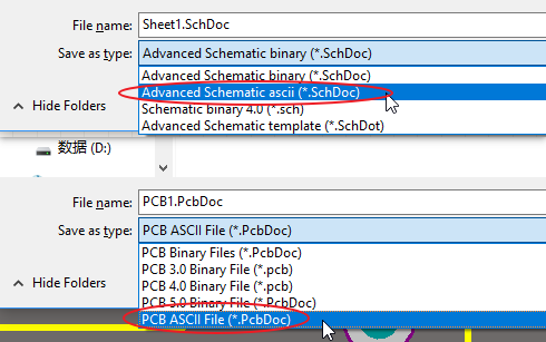
- Select "Save As"
- Select ASCII format from the drop-down list of document type: PCB ASCII File(*.PcbDoc) or Advanced Schematic ascii(*.SchDoc)
- save.
If it is a Protel 99se file, please open it in Altium Designer first, then save it according to the above method, and then import it.
Import Alitum library file
Since Altium Designer schematic library files and footprint library files do not support saving in ASCII format, EasyEDA does not support direct import of Altium Designer library files.
You can put all the library files you need to import in the schematic diagram or PCB, then save the schematic diagram and PCB in ASCII format, and then select "Extract library files" to extract all the library files when importing. After extraction, it can be directly placed on the corresponding canvas, or directly added to the personal library. 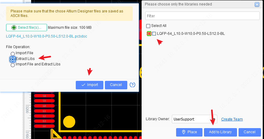
Batch convert ASCII files
How to batch import existing schematics, PCBs and library files in Altium Designer:
Download EasyEDA Pro format converter for format conversion.
or Altium script. export-altium-to-ascii.zip
Extract the currently installed library files to the schematic diagram or PCB according to the script tutorial.
Compress the generated schematic diagram or PCB file into a zip archive, import it, and extract the library. First extract the footprint library and then extract the symbol library.
After importing, find the extracted library at "Left Component Library - Symbol/footprint - Workspace".
common problem
The difference before and after format conversion is as follows:
Schematic / component library:
| Elements/Layers | After Import | Notes |
|---|---|---|
| Pictures | Import is not supported | AD pictures are stored in local file paths, and ASCII files do not contain pictures |
| Off Sheet Connector | does not support import | standard version does not support off-map connector |
| Sheet Symbol | Import not supported | Standard version does not support page breaks |
| Sheet Entry | Does not support import | Standard version does not support drawing entry |
| Device Sheet symbol | Does not support import | Standard version does not support device page symbol |
| Harness | Import is not supported | Harness entities are not supported in Standard Edition |
| Directives | Import is not supported | The standard version supports No ERC labels, and does not support other indication entities (differential pairs, parameter settings, coverage areas, compilation shields) |
| Text/Text Box/Comment | Import as normal text | The standard version does not support comments. If the corresponding font is not installed in the operating system, the original font will be used first after the text is imported, and the default font will be used if it cannot be found (determined by the browser) ), there may be a slight offset due to different fonts of the text; when the AD file is saved as ASCII, Chinese characters may be garbled, and the garbled characters will be automatically converted to underscores after import |
| Component tag | Multi-part tag U1A, U1B after import is U1.1, U1.2 | The standard version does not support multi-part tag like AD |
| Pin type | Unsupported types are uniformly converted to undefined types | The standard version only supports four pin electrical types |
| Hidden pins | Show after import | Standard version does not support hidden pins |
| Component Designator | After importing, "original footprint 1, original footprint 2, etc." will be generated | The standard version is not associated with the footprint name, but is based on the uuid of the footprint, so when importing, multiple footprint names that are originally associated will be added as common attributes , if the imported schematic and PCB are compressed and imported together, the footprint will be automatically associated |
| Theme style | The import dialog uses the default theme of the source file | Import the theme of the original file |
| IEEE symbols | IEEE symbols are not supported for import | AD IEEE symbols are not supported for import |
PCB/Footprint Library:
| Elements/Layers | After Import | Notes |
|---|---|---|
| polygon pour | polygon pour will be re-laid after importing | Because the polygon pour logic is different, the polygon pour filling of the PCB will also be slightly different. For example, the generation method of heat welding, the width of heat welding, and whether there is an extra part of heat welding may cause flying lines; horizontal and vertical polygon pour will be converted to grid polygon pour; AD grid polygon pour will heat and weld the vias separately, The standard version does not support it, and some vias may not be connected to the copper layer after rebuilding the copper layer (when the grid is relatively large); the standard version does not support the copper layer of the non-signal layer, so the copper layer of other AD layers will be converted to polygon pour on the top layer |
| Design rules | Some design rules do not support import | For example, custom advanced design rules, design rules not supported by the standard version, common safety spacing, etc., the parameters of the imported PCB file rules need to be adjusted by themselves |
| Text/Text Box | Font changes and positions will be slightly offset | After the text is imported, the default font will be used (Chinese uses Google fonts), and the position of the text may be slightly offset due to the font of the text; if it is the same font, because the font The displayed logic is different and cannot be completely consistent with the original file, there will be position offset and size difference; strokes and barcodes will be converted to ordinary text |
| Internal electrical layer | The network of the block may change after importing | The implementation of the internal electrical layer of AD and the standard version is different. When there are multiple internal electrical blocks, the network of the blocks may not be completely consistent, so you need to be careful Check; the internal electrical layer will rebuild the block after importing, and the internal electrical layer block division may also be different |
| keepout layer | is converted to frame layer by default | In the import pop-up window, it is supported to set whether the source of the frame is the keepout layer or the mechanical layer 1; the keepout closed lines inside some boards will automatically be converted to the corresponding forbidden area according to the target; Closed keepout primitives will be imported to the mechanical layer, and the standard version does not support independent lines as forbidden areas |
| Board shape | Go to the document layer by default | The standard version does not have a board shape but has a border layer. Since most people use keepout and mechanical layer 1 as the board frame, the board shape goes to the mechanical layer |
| Define Board Cutout | Convert to slot | This function corresponds to the standard version of the solid filled slot type |
| Polygon pour Cutout | Convert to Solid Fill No Fill Type | Convert to Solid Fill No Fill Type |
| Mechanical layer | Mechanical layer 1 is transferred to the mechanical layer by default, and other mechanical layers are transferred to the document layer | The standard version does not support the functions of other mechanical layers |
| Ratlines | Flying lines appear after importing | It may be that the reconstruction of polygon pour after importing leads to disconnection in some places, such as no network primitives, heat welding cannot be generated due to DRC spacing, etc. |
| Room | Does not support import | Standard version does not support Room primitives |
| Layer stack settings | Import is not supported | Layer stack settings are not supported in Standard Edition |
| 3D body/3D model library | Does not support import | The 3D binding design of the standard version is different from AD |
| Drill table | Import to mechanical layer | Drill layer not supported in standard version |
| Solder mask and flux extension of primitives | Only pad vias support import | Solder mask and flux extensions of other primitives, such as wires and arcs, do not support import |
| Pad | Import to the bottom layer or top layer or multiple layers | The pads of the standard version do not support being set on any layer, and the pads of the unsupported layer will be converted to the filling area of the corresponding layer; the rectangular drilling is not supported, and will be converted to Groove Drilling |
| Component/footprint | Import to the top layer or bottom layer | If the footprint attribute drawn in AD is on the top layer, but the whole is on the bottom layer (belonging to wrong data), it will automatically correct the layer attribute to be on the bottom layer after importing |
| Coordinates | Import as Text and Lines | Coordinate entities are not supported in Standard Edition |
| Dimensions | Partially supported for import | Partially supported for import as text and lines |
| Object from file | Import not supported | This calls an object outside the file, not contained in the file, and does not support import |
| Work Guides | Import Not Supported | Standard Version Does Not Support This Element |
Other frequently asked questions:
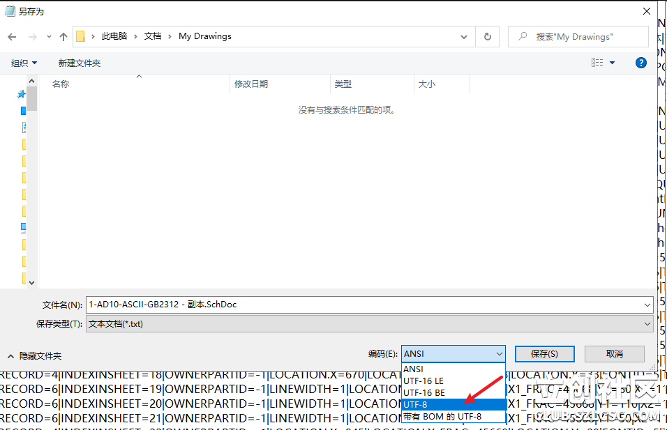
- Chinese garbled characters appear when importing AD schematic In versions below AD17, the encoding of the ASCII file saved as may be GBK2312, and the encoding of the ASCII file needs to be converted from GBK2312 to UTF-8. You can save as a UTF-8 encoded file using a text editor. method:
- Use AD17 to save as ASCII file, the default is UTF-8 encoding
- Or use the system notepad to open the ASCII file, and select UTF-8 encoding when saving as. Other text editors also have corresponding encoding conversion functions.
- Or use the system notepad to open the ASCII file, and select UTF-8 encoding when saving as. Other text editors also have corresponding encoding conversion functions.
- After importing the AD file, there are wires and device pins that are not aligned with the grid, or the pins are biased
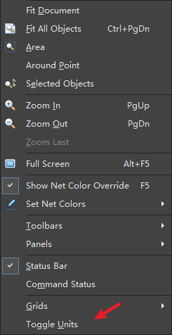
- First set the unit of the schematic diagram in Altium Designer to imperial mil, in: view menu - switch unit
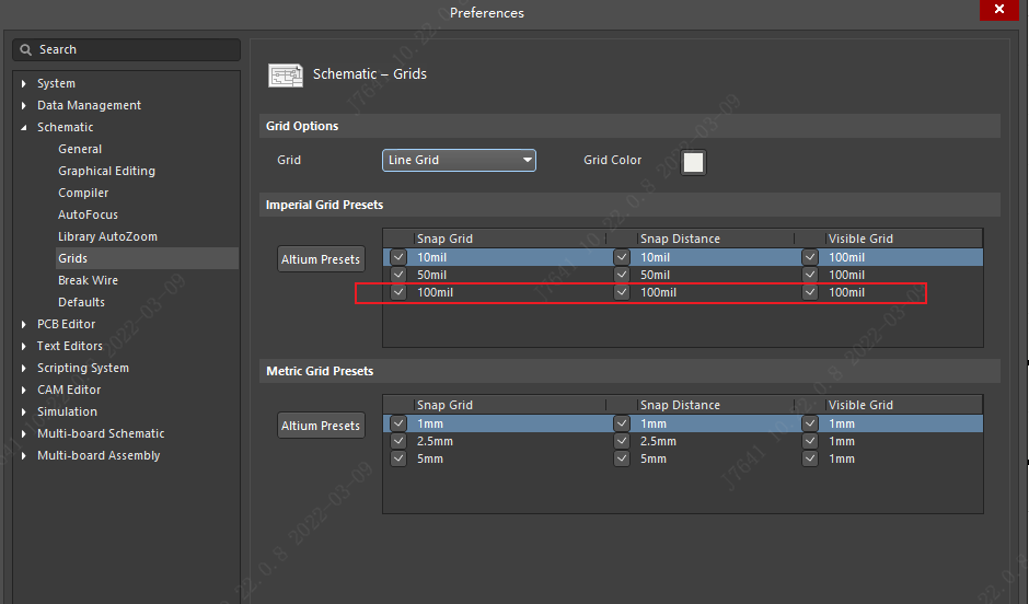
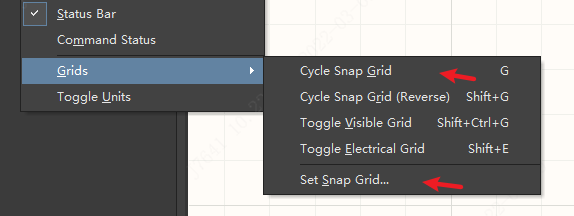
- Then the canvas right-click menu or system settings: Options - Grid - set the display grid, electrical grid, adsorption grid to 100mil, switch grid to 100mil
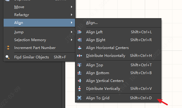
- Select all schematics CTRL + A , use Edit menu: Edit - Align - Snap to Grid function. Check for broken or wrong places to correct.
- Save as ASCII and import
Please do not repeat your original Schematic or PCB exported to AD format and then imported, this operation may lead to loss of details! ! !
When importing Altium files, if there are unsupported characters (such as garbled characters), they will be automatically converted to underscores, so after importing, you may find that there is an extra underscore in network labels, device names, footprint names, attributes, etc. Please modify it manually . When the current version of AD is saved as an ASCII file, the Chinese will become garbled, so it is also garbled when imported. You need to open the ASCII file with a text editor such as Notepad and then import it after correction.
The maximum size of the imported AD file is 100MB. The larger the file size, the longer the import time will be or the import will fail. It is recommended to manually reduce the file size. For example, delete the copper filling first (set the copper filling to no filling type) and then import.
Eagle Schematic/PCB/Library
Please look at the chapter
KiCAD schematic/PCB/library files
Please see the next chapter
LTspice schematic file
Because EasyEDA has rewritten the conversion code for file import, the import of LTspice files needs to be redeveloped, and it has not been developed yet, and the import is not yet supported.