UI Introduction
EasyEDA Editor has a clear and friendly user interface. It has a short learning curve, and you will be productive in a short time.
Filter
To use the filter first select what module you need in the left navigation panel, and then you can find projects, files, parts, and footprints quickly and easily just by typing a few letters. For example, if you want to find all files containing “NE555” in the title, just type “555”. The filter is non-case sensitive. 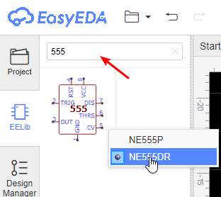
The Filter can only find projects, files, part titles, and names. It does not search the Descriptions and Content fields.
Click the X to clear the filter.
Navigation Panel
The Navigation panel is especially important for EasyEDA: This is where you can find all of your projects, files, parts and footprints.
Project
Here you can find all your projects, both private or shared with the public, or fork them from someone else's. These options have a context menu found by right clicking and selecting Projects. You will get a menu tree like: 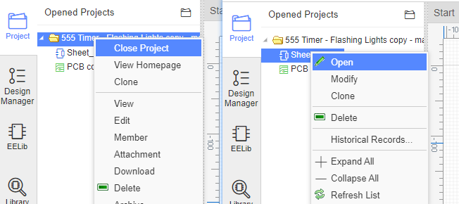
Commonly Library
Commonly Library means EasyEDA Libraries, it provides lots of components complete with simulation models, many of which have been developed for EasyEDA to make your simulation experience easier.
Design Manager
Design Manager, you can check each component and net wiring, and it provides DRC(Design rule check) to help improve your design. 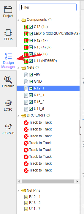
Library
Contains schematic symbols and PCB footprints for many available components and projects. Your own libs and modules will show up here. 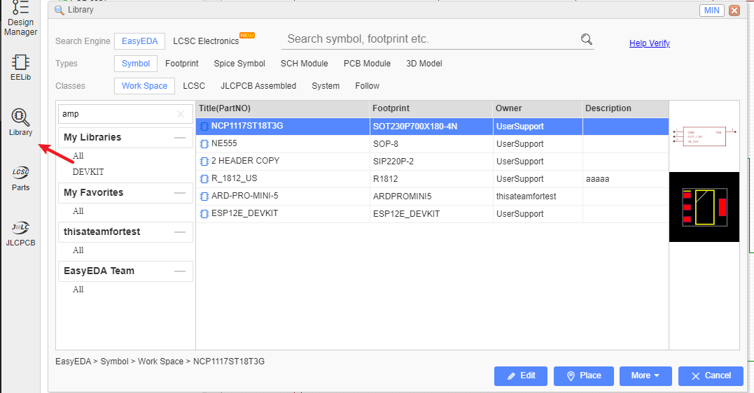
LCSC If you want to buy components to finish your PCB, you should try the LCSC module. LCSC.com and EasyEDA are the same company. EasyEDA partners with China's largest electronic components online store by number of customers and product quantity shipped. https://lcsc.com. LCSC means Love Components? Save Cost! We suggest to our users to use LCSC parts to design. Why?
- Low minimum required quantities & Global Shipping.
- More Than 25,000 Kinds of Components.
- All components are genuine high quality.
- Ordering components is easy.
- Savings can exceed 40%.
- You can use LCSC component symbols and footprints directly in EasyEDA editor.
JLCPCB JLCPCB.com, LCSC.com and EasyEDA are all part of the same company group. https://jlcpcb.com More than 200,000 customers worldwide trust JLC, 8000 + online orders per day, JLCPCB (Shenzhen JIALICHUANG Electronic Technology Development Co.,Ltd.), is the largest PCB prototype enterprise in China and a high-tech manufacturer specializing in quick PCB prototype and small-batch production. Affordable, high quality boards ae fully manufactured in China. Boards are fully e-tested. Pricing is clear and easy to understand.
Top Menu
Most EasyEDA features can be found on the top menu: 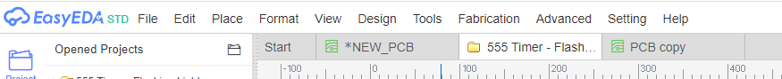
You can find what you need easily and clearly.
Preview Dialog
The Preview dialog will help you choose components and footprints and can help you to identify schematics and PCB layouts.
You can close or open this dialog with:
Top Menu > View > Preview Window. 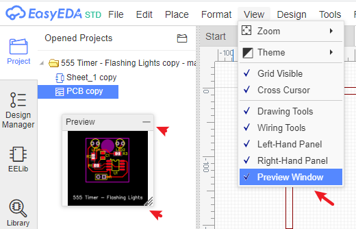
- The Preview Dialog has a resizing handle in the bottom right corner.
- The Preview Dialog can't be closed but double clicking on the top banner will roll up the panel or you can click the top right corner
—. Double clicking the top banner again toggles it back to the selected size.
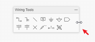
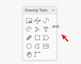
Wiring Tools
The Wiring Tools are document type sensitive: different document types have different tools.
Drawing Tools
To keep EasyEDA's UI clean and sharp, the Wiring and Drawing tools palettes can be resized horizontally, rolled up or hidden so if you want to focus on drawing or have a smaller monitor, you can roll up or hide them to free up more monitor space and reduce the clutter.
Canvas Attributes
You can find the canvas Properties setting by clicking in any blank space of the canvas.
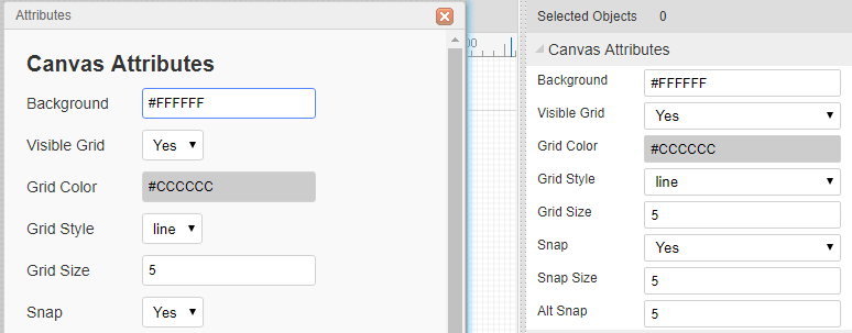
The background and grid colors and the style, size, visibility and snap attributes of the grid can all be configured.
The canvas area can be set directly by the Width and Height or from the available preset frame sizes.
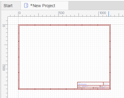
Canvas
This is where it all happens! This the area where you create and edit your schematics, PCB layouts, symbols, footprints, and other drawings. You also run simulations and display Waveform traces from here.