Board Outline
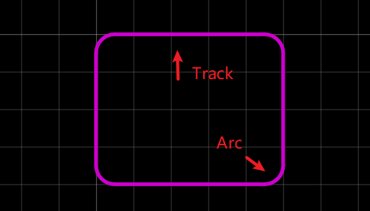
Before placing footprints we need to create a board outline. The board outline must be drawn on the Board OutLine layer. So first, set Board OutLine as the active layer, then draw the board outline using Track and Arc from the PCB Tools palette.
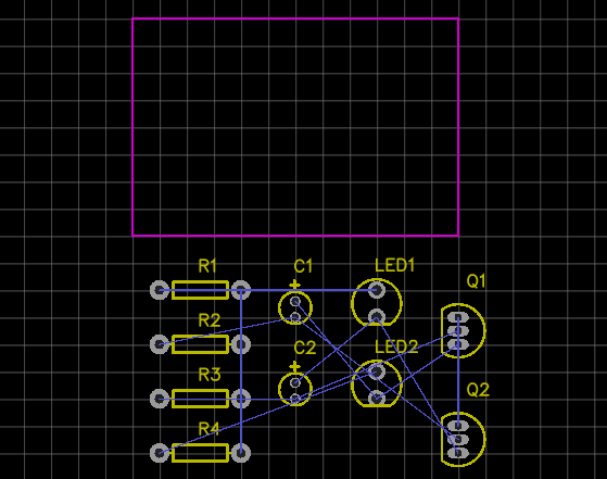
When converting a Schematic to PCB, EasyEDA will try to create a board outline for you.
The area of the default board outline area is 1.5 times the sum of the area of all of your footprints, so you can place all of your footprints into this board outline with some allowance for tracking. If you do not like the board outline, you can remove the elements it is made up from and draw your own.
To create a simple rectangular board outline, this arc can be removed and the line X and Y end points edited - either directly in the Properties panel or by dragging the line ends - to close the rectangle.
And EasyEDA provides a Board outline wizard, so it is very easy to create a board outline. Via: Top Menu > Tools > Set Board Outline, Or find it on the toolbar.
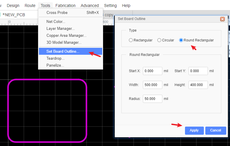
In this dialog, there's a choice of 3 types of board outlines, Rectangular , Circular, Round Rect. If you need a different more complex board outline, you need to import a DXF file.
Notice:
- When generate the Gerber, EasyEDA will show error if the board outline doesn't closed or the board outline tracks overlap.
- You can cutout the hole by using the board outline, or use
Hole, orSolid Region(Type: Board Cutout)to create the hole instead of using the board outline. - You can right-click track or circle to convert to board coutout.
- If the board outline doesn't closed, the copper pour will not show up.