Design Rule Check(DRC)
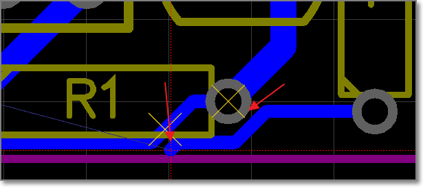
EasyEDA provides a real time DRC(Design Rule Check) function. This is a big feature of EasyEDA. It is hard to fix DRC errors after laying out the PCB. Now EasyEDA will let you know the error in routing. You will find an X flag to mark the error.
Design Rule Setting
Via at: Tools > Design Rule..., or Via: right-click the canvas - Design Rule... to open the Design Rule setting dialog:
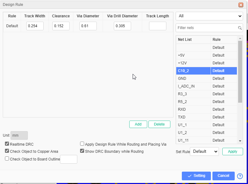
The unit follow the canvas unit.
Rule: The default rule named "Default", you can add the new rule you can rename and set parameters for it. Each net can be set a rule.
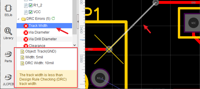
Track Width: Current rule's track width. The PCB track width can not less than this value.
Clearance: The clearance of different objects which have different net. The clearance of the PCB can not less than this value.
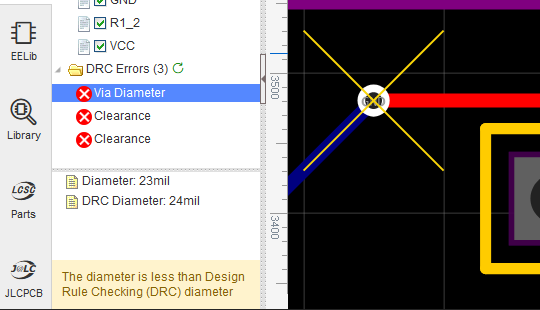
Via Diameter: The via diameter of current rule. The via diameter of the PCB can not less than this value. Such as the Hole/Multi-layer Pad's diameter.
Via Drill Diameter: The via drill diameter of current rule. The via drill diameter of the PCB can not less than this value.
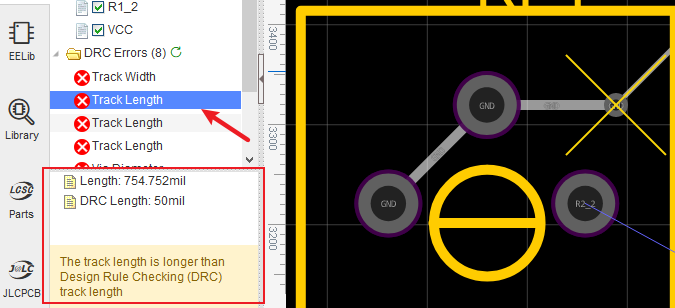
Track Length: All track length of current rule. The length of tracks belong to a same net should not be longer than this value.Including the arc lenghth. When the input box is empty the length will be unlimited.
Realtime DRC: After enable, when you routing the DRC will checking all the time, when appear the error the canvas will show the "X" marking.
Check Object to Copper Area: Check the clearance of the objects to copper area. If you disable this option, you must rebuild the copper area before generating the Gerber with SHIFT+B.
Check Object to Board Outline: When you enable, you can set a value to check the clearance of the objects to board outline.
Apply Design Rule while Routing and Placing Via: When you routing and placing a new via, them will follow the design rule to set them width and size.
Show DRC Boundary while Routing: When routing you will see a oultine around the track. Its diameter depends on desgin rule.
Set Rule for a Net
- Click the "new" button to create a rule, or use the default rule
- Select one or more networks on the right, support holding down the CTRL key for multiple selection, and also can perform keyword filtering and rule classification filtering
- Then select the rule you want to set in the "set rules" section below and click the "apply" button. The network applies the rule.
- Click the "Settings" button to apply the rule.
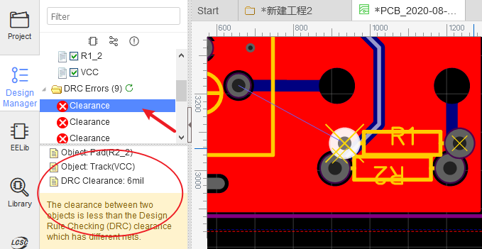
Check the DRC Error
Via "Design Manager - DRC Error" or "Top Menu - Design - Check DRC", click the refresh icon to run the DRC. If your PCB is a big file, and have the copper area that will take some times to check the DRC, please wait a while. 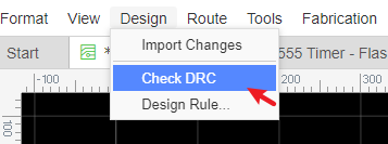
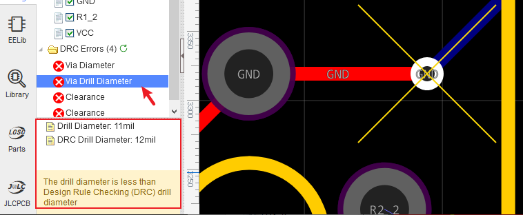
After checking, you can view all the error at the "DRC Error", click the error the related objects will be highlighted. 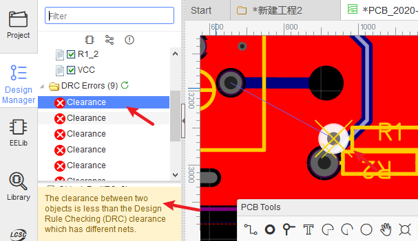
DRC error type
Clearance: Object to Object. If two different net objects too close, and the distance less than the Design Rule clearance, it will show the Clrearance error.
Track Length: The track Length of the all same net tracks must less than Design Rule track Length.
Track Width: The track width must must large than Design Rule track width.
Via Diameter: The via diameter must large than Design Rule diameter.
Via Drill Diameter: The via drill diameter must large than Design Rule drill diameter.
Note:
- When you convert a schematic to PCB, the real time DRC is enable. But in the old PCB, the real time DRC is disable. you can enable it in the image as above.
- Design rule checking can only help you find some obvious errors.
- The color of the DRC error can be set in the layer manager.