Layer Manager
Layer Manager
You can set the PCB layer's parameters at the Layer Manager.
Via Top Menu> Tools > Layer Manager..., Or Click Layers Tool gear icon. Or right-click the canvas - Layer Manager menu.
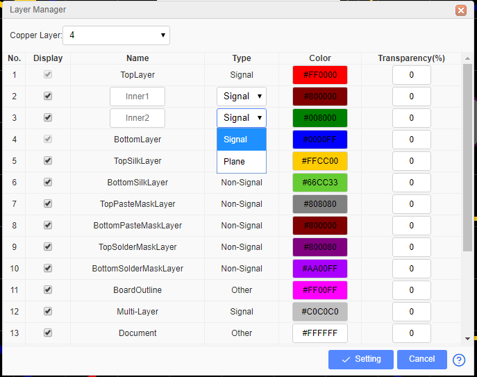
The Layer Manager dialog:
The Layer Manager setting only works for the current editing PCB.
Copper Layer: The copper layer of your PCB. EasyEDA support 34 copper layers. The more copper layers the PCB will be more expensive. The TopLayer and BottomLayer is default layer, can not be disable. If you want change the copper layers from 4 to 2, you must delete the inner layers objects first.
Display: If you don't want a layer dosen't display at "Layers Tool", you can disable the checkbox. Notice: This option only hide the layer name on the "Layers Tool", the objects of the hidden layer still exist, when you generating the Gerber, they will appear.
Name: Layers name. For the inner layer, you can define the name.
Type:
- Signal: Which is working for the signal. Such as Top and bottom layer.
- Plane: When the inner layer type is "Plane", this layer will be copper pourred, if you want to separate the copper area you can draw the Track or Arc. You can treat this layer is a only has the copper area, but its easy than draw the copper area. The track you routed will generate the clearance when generating the Gerber. The "Plane" usually is using for the Power or Ground copper pour on the inner layer. You can set the net for the plane zone.
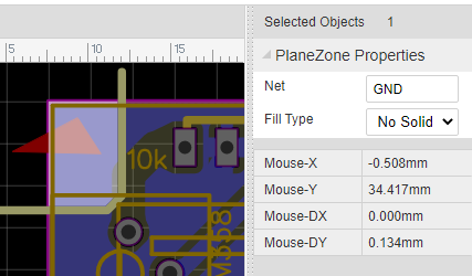 Notice: When draw the track to separate the plane zone, the track start ponit and end point must over the middle line of the board oultine track. Otherwise, the plane zone will not be separated; When using the plane layer, the PCB can not exist two closed borad outline, only one closed board outline will generate the plane zone.
 - Non-Signal:Such as silk screen, mechanical layer, document layer etc.
Color: You can define the color for each layer.
Transparency: You can change the layer transparency.
Layer Definination:
- TopLayer/BottomLayer: The top side and bottom side of the PCB board, copper layer.
- InnerLayer: Copper layer, routing track and copper pour.
- TopSilkLayer/BottomSilkLayer: Board silkscreen.
- TopPasteMaskLayer/BottomPasteMaskLayer: This layer is the layer used to make the stencil for the SMT pads, helping to solder. This layer has no effect on production if the board is not required to make the stencil.
- TopSolderMaskLayer/BottomSolderMaskLayer: The top and bottom cover layers of the board are typically green oil, which acts to prevent unwanted welding. This layer belongs to the negative film drawing mode. When you have wires or areas that do not need to cover green oil, draw them at the corresponding positions. After the PCB is generated, these areas will not be covered with green oil, which is convenient for operations such as tinning.
- BoardOutline: The board shape definition layer. To define the actual size of the board, the board factory will produce the board according to this shape.
- TopAssemblyLayer/BottomAssemblyLayer: Simplified outline of components for product assembly and repair. Used to export document printing, without affecting PCB production.
- MechanicalLayer: Record the information on the mechanical layer in the PCB design, and only use it for information recording. By default, the shape of the layer is not manufactured at the time of production. Some board manufacturers use the mechanical layer to make the frame when using Altium file to production. When using Gerber file, it is only used for text identification in JLCPCB. For example: process parameters; V cut path etc. In EasyEDA, this layer does not affect the shape of the border of the board. If the mechanical layer has closed wires, JLCPCB will give priority to using the mechanical layer as the shape of the board when producing the board. If there is no outer frame of the mechanical layer, GKO will be used as the frame (historical influence of Altium file). It is necessary to pay attention to the use of the mechanical layer in the design.
- DocumentLayer: Similar to the mechanical layer. But this layer is only visible in the editor, when in the Gerber file it doesn't join into fabrication.
- RatlineLayer: PCB network ratline display, this layer is not in the physical sense, in order to facilitate the use and set color, it is placed in the layer manager for configuration.
- HoleLayer: Similar to the RatlineLayer. For Hole(Non-Plated Hole) display.
- Multi-Layer: Similar to the RatlineLayer. For multi-layer hole(Plated hole) display. If the PAD setting layer property as mult-layer, it will connect with all copper layers.
- DRCErrorLayer Similar to the RatlineLayer. For DRC(Design Rule Error) marking dispaly.
Layout Single Layer PCB
The PCB copper layers of EasyEDA are double, EasyEDA doesn't support layout a signle layer directly. if you want to layout a single layer PCB(such as only layout on the bottom layer),
There are two methods:
Method:
- Layout and route directly on a single layer (top or bottom layer) without placing vias.
- If you are using a footprint with multi-layer pads, you can keep the inner wall of the hole metallized as needed. At this time, you can find all the multi-layer pads by Find Similar Objects. If you do not need the inner wall of the plug-in pad hole to be metallized, you can change the metallization ( plated) attribute of the pad to No, and retain the metallization. Can streng then welding.
- After generating Gerber, delete the unnecessary layer files (for example, if you only need the bottom side layer, you need to delete the Top-related files Gerber_TopLayer.GTL, Gerber_TopPasteMaskLayer.GTP, Gerber_TopSilkLayer.GTO, Gerber_TopSolderMaskLayer.GTS), and recompress them into zip That’s it.