Panelize
via: Top Menu - Tools - Panelize
Panelize by Editor
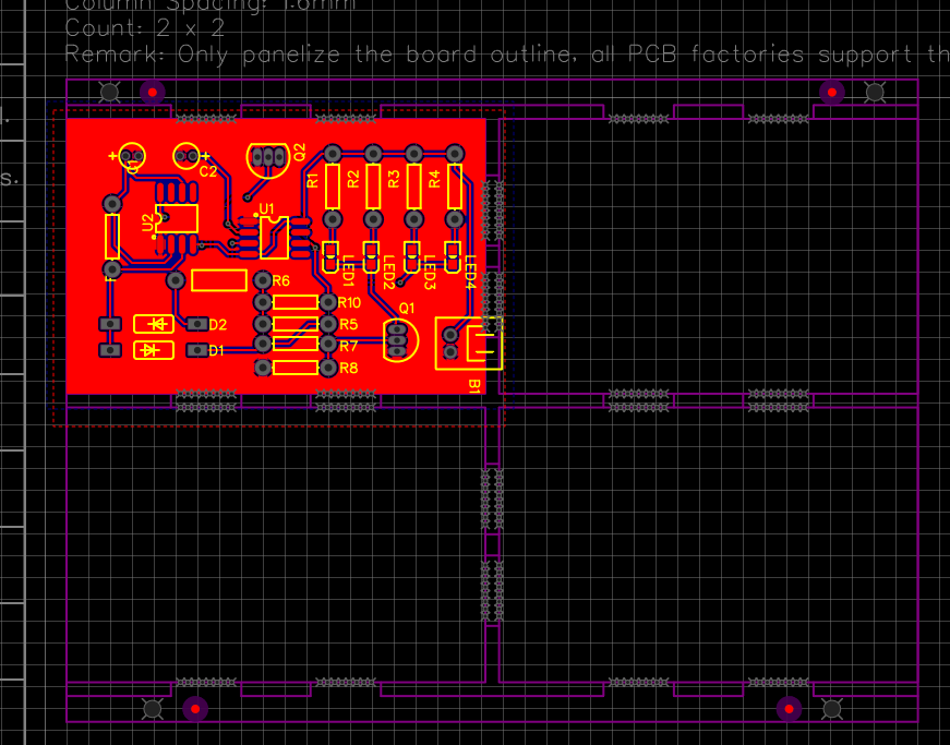
At present, EasyEDA only support to panelize PCB itself, in order to decrease the file size, the panelized file only panelize the board outline. Normally, all the PCB factory will support this panelized file, if you not sure, you need to contact your PCB factory support.
via: Top Menu - Tools - Panelize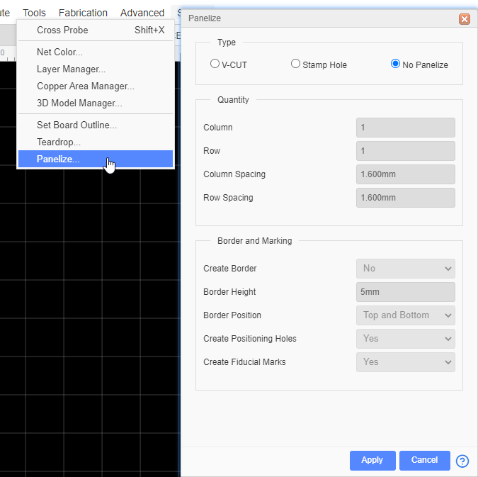
The Border height can not less then 3mm.
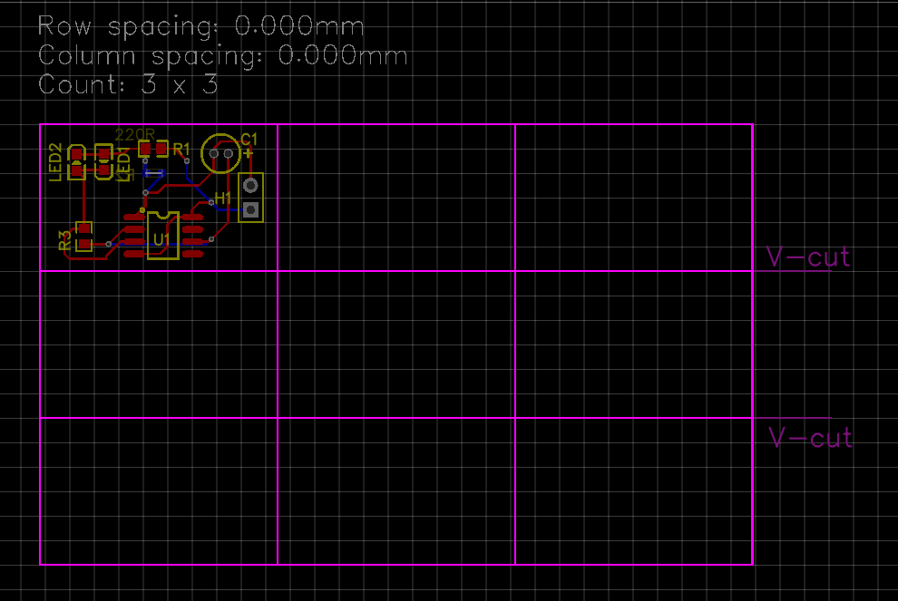
V-cut: If you choose V-Cut, the editor will add the v-cut indication track on Board Outline layer at the Gerber.
Stamp Hole:
When you preview the Panelize Gerber at JLCPCB.com, you will get the image like below:
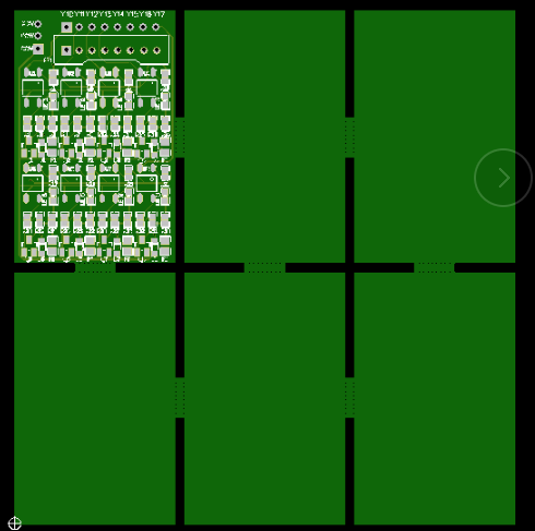
JLCPCB will take care of your design, they know how to do.
Panelize by Manually
Process:
- Select the whole board, hotkey
CTRL+A. - Copy the whole board by reference point, hotkey
CTRL+SHIFT+CorCTRL+C. You can only copy and paste the board outline to become the panelize board. - Paste the board via hotkey
CTRL+SHIFT+V, this hotkey will keep the prefix and hide the ratline layer. - Paste repeatly, after finish, rebuild the copper area with
SHIFT+B, recommend draw copper area at the end.
Notice:
- The board with an internal plane layer cannot be used by manual panels, otherwise the inner electric layer cannot take effect normally.Because the implementation method of the internal plane layer must be available with the full border, manually copying and paste multiple borders in the border's internal plane blocks will be abnormal, and the network cannot inherit. It is necessary to change to the signal layer with copper instead of internal electricity segmentation.
- The editor's own panel and manual panel cannot be performed at the same time.