Solid Region
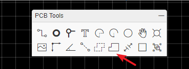
EasyEDA has added a new tool Solid Region for PCB design
This is a very useful, quick way to connect Pads. You can draw a Solid Region to include all of these pads with same net name, then set the region to the same net name as the pads. It is like Copper Area but easier to use for small areas. To use Solid Region like this, set the Type attribute (in the right hand Properties panel) to Solid.
When you drawing the solid region, you can use the hotkey L and space to change the route type(Arc, 90 degrees, 45 degrees, Free Angle), just like the track routing.
When you finish drawing, you can click the solid region and change its attributes at the right-hand panel. 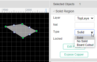
- Layer: Solid Region su pport many layers, you need to enable the layer at the Layer Manager first.
- Net: When change to top or bottom or other inner signal layer, the solid region can be set a net to connect other objects. Sometimes, you can use solid region to make the copper instead of "Copper Area".
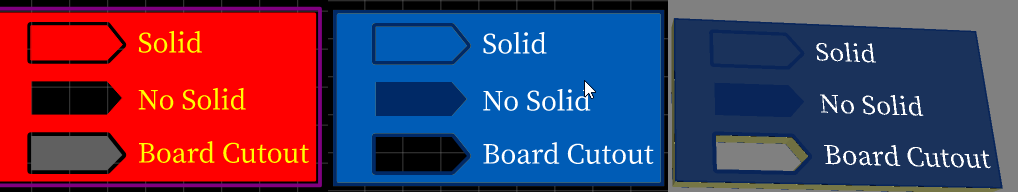
- Type: Solid,Board Cutout,No Solid , - Solid: It will fill the solid area. - No Solid: It will cutout the area such as copper area. Notice, if you cutout a copper area, the solid region's net must different than copper area's net. After setting to this option, you need to rebuild the copper area with SHIFT+B. - Board Cutout: you can use this feature to create a slot hole(Non Plated Through Hole).
- Edit Points: You can edit the solid region's outline points as you want.
- Expose Copper: ou can create an aperture in the solder mask by one click. It's very easy to do.
The outline of the solid region can not be self-intersection, when it happens, please delete the self-interation point at "Edit Points".