Create The Footprint
Create The Footprint
There will be times when you will need a PCB footprint that is not already in the EasyEDA libraries.
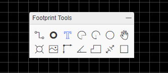
Footprint Tool
The process of creating your own Footprints is very similar to how you make symbols for your own Schematic Libs.
Footprint Tools almost are the same as PCB tools, just lacking some of the functions.
Create Footprint
Start a new Footprint as shown below or by doing:
File > New > Footprint
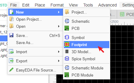
This opens the New Footprint editor.
Drawing Steps
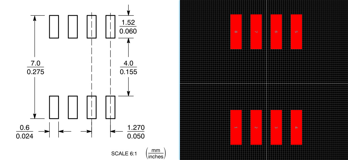
1.Downlod the datasheet which you need to draw the Footprint, such as SOIC-8.Such as PDF:UC2844BD1R2G
2.Read the datasheet, notice the 0 degree of the Footprint (The 0 degree is the Footprint's direction when you placed it on the PCB without rotation), the right 0 degree will helpful for PCB SMT.
3.Check the footprint size, pad/pin direction and polarity, and then place the Pads on the canvas. You can adjust the pad size base on your real usage situation.
- Component's pin direction, page 1.
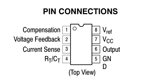
- footprint polarity, page 1 and 18.
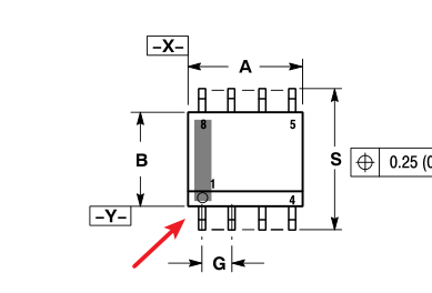
- Depends on page 18, placing one pad on the canvas on the top layer, and then change the pad number, size, shape type etc. And then set the coordinate for it, and place the less pads, you can use the "Top Menu - Align" tools to align the pads to fit the location. If you want to move the pad by mouse or direction key by small steps, you can set a new snap size at the right-hand panel.
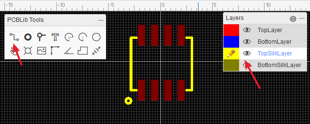
4.Drawing the Footprint silk screen. And sometimes you can add some marking and text on the mechanical or document layer.
- Swicthing layer to TopSlikLayer
- Using the Track and Arc to draw the silk screen. The editor doesn't support draw the retangle silk screen at present.
5.Filling the footprint title and prefix at the right-hand "Custom Attributes", and then Save. When you save it , please fill the tags, description, the description suggesting add the footprint datasheet link and footprint size, that can help you or other people to recognize this Footprint whether if it can be used for the design. 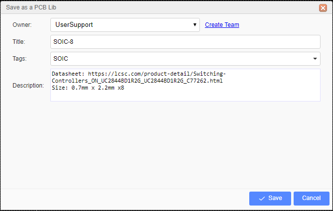
6.Use the dimension tool to check the Footprint size, via: Top Menu - Tools - Check Dimension.
7.Set the origin. You can via: "Top Menu - Place - Set Canvas Origin - By Center of Pads" to set the origin.
8.Save.
Then the PCB footprint creating finish .
Notice:
- The Origin Point. To simplify rotating your symbols when they are placed into the canvas, make sure all of your symbols are created as near as possible centered around that point. Suggesting the footprint center to be the origin point. That will helpful to rotation when you placing it on the canvas, and help to do the SMT more quickly.
- The pad center suggesting one and more on the grid , avoid when place it on the PCB causing the track hard to connect issue.
- The pad number can be set as number and alphabet, they must match with the SchematicLib's pin number, otherwise the component which was assigned this Footprint will alert the error at the footprint manager, and can' not convert the schematic to PCB.
- The pad number will increase by placing with mouse, if you copy and paste it, the number will not increase.
Others
It is important to set the right Snap and Grid sizes to ensure that the pads on the finished footprint snap exactly to the grid and so connect the nets. For example, if you are creating a DIP footprint, set the Grid size to 100mil.
Keep all other shapes such as component outlines and any associated pin identification marks or text on the TopSilkLayer. EasyEDA will automatically take care of the actual layer assignment when you place the footprint on the PCB.
CTRL+Sto save your footprint designs and you will find them saved into the Libraries > Classes: Footprint > Personal > Created section of the left Navigation panel.Annular ring of the pad/via is too small, keep the annular ring >= 4mil. In this case, you can add a
Hole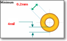
Pad attributes
You can add pads using the Pads button from the Footprint Tools palette or using the P hotkey.
After selecting one of the pads, you can view and adjust its attributes in the right hand Properties panel. 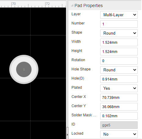
Number: Remembering the pin numbers you set in the schematic symbol in your Schematic symbol: to connect those schematic symbol pins to the pads in your PCB footprint, the pad numbers you set here in the Footprint footprint must be the same.
Shape: Round , Rectangular , Oval and Polygon.
EasyEDA supports four shapes: Round , Rectangular , OVAL and POLYGON.
OVALPAD will give your more space.POLYGONPAD will let you to create some strange pad.
Like in the image below, you can edit the PADs points when you select a POLYGON PAD 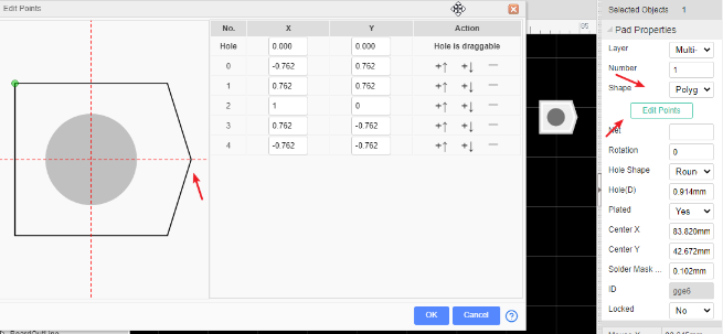
Layer: If the pads are part of a SMD footprint, you can set it to Top layer or Bottom layer. For through hole components you should set it to Multi-Layer.
Net: You don't need to enter anything here because at present this footprint is not connected to anything in a circuit.
Width and Height: When the shape is set to Round, Width will equal Height.
Rotation: Here you can set the Pad's rotation as you want.
Hole(D): This is the drill hole diameter for a through hole pad. For a SMD Pad, set this to zero.
Center-X and Center-Y: using these two attributes, you can set the pad's position with more precision, compared to using the mouse.
Plated: Yes or No. when the pad is multi-layer pad, if it set the plated as no, this pad top side and bottom side will not be connected together.