Edit Footprints
Edit Footprint in Library
When you found a Footprints(footprint) but it can not be satisfied for your design, you can edit it to be your personal PCB footprint.
Via Library > Footprint > Search Component/Personal/LCSC/System > Select footprint > Edit
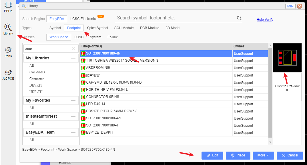
You can edit the pad size, shape outlines, etc. when you finish and save, it will be saved to your personal libraries "Created" and become your personal libraries.
And you can add a tag for your Footprint when you save it: 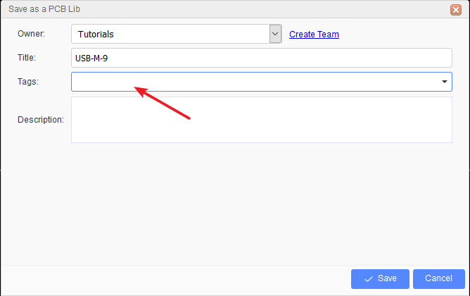
Modify the saved Footprint tag at "Library" part list. 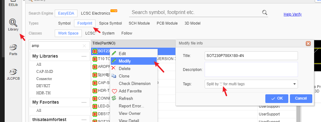
Edit Footprint in PCB
If you want to edit a package(footprint) in the PCB, you can use the Ungroup/Group function same as the schematic.
On the PCB Tools palette there is the Group/Ungroup Symbol… button.
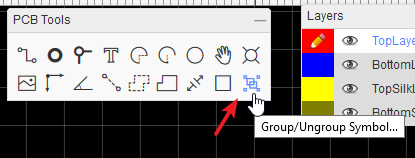
This tool is for you to quickly create or edit library symbols.
Select a footprint
Click the Group/Ungroup Symbol… button Up to this point you have a collection of separate pads, a drawn silk layer tracks and some text that are all separate items with no particular association with each other.
Edit the shape or pad what you want to change
Select all of the items and click the Group/Ungroup Symbol… button.
A dialog will be opened:
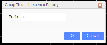
After you click OK, all those separate elements will be grouped together to form your new symbol directly in the PCB.
Using the group function, you can create/edit any symbol in the Schematic/PCB, easily and quickly.
Notice:
- Before ungroup the footprint, please change it's layer to top layer first, because of the footprint after grouping will at top layer.