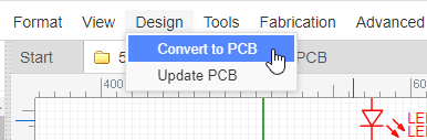
Convert Schematics to PCB
Convert to PCB
Most of the time, schematics are created with the aim of producing a PCB. So how do you convert your schematic to a PCB in EasyEDA? You just need to to click the PCB icon on the toolbar with the title Convert to PCB.
Note:
- Before converting, you need to use the Design Manager and Footprint Manager to check all the components, nets(connection) and footprints to ensure no errors exist.
Footprints Verification
After clicking the Convert to PCB button, if the project has errors the following dialog will open: 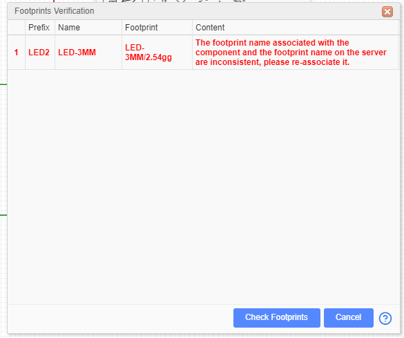
The row in red indicates that EasyEDA can't find a PCB footprint matching the footprint that the schematic symbol is calling for.
This could be because you have made an error entering the footprint attribute in the symbol's Properties or maybe you haven't yet created a PCB footprint for the footprint that your symbol is calling for.
In this case the footprint should have been AXIAL-0.3 but instead it is empty. To correct it you can click on the row and update the footprint AXIAL-0.3 for it at the footprint manager.
After making any necessary corrections, click the Convert to PCB button and EasyEDA will automatically load all the PCB footprints into the PCB editor as shown in the image below.
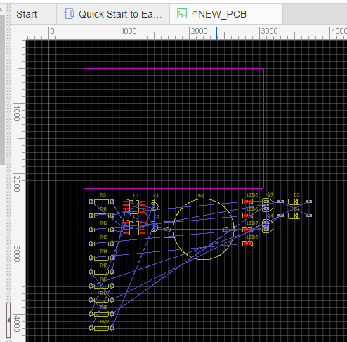
This shows the footprints placed in arbitrary positions with the connections between them shown as blue Rat lines.
Invalid footprint
The footprint's PAD number is different from the symbol's PIN number, e.g. the diode footprint's PAD numbers are A,C but the symbol's PIN numbers are 1,2. You just need to change one to fit the other. It is case sensitive!
the changing method please refer the Schematic - Footprint Manager section.
Update PCB
Converting a schematic to PCB can be done using the Convert to PCB... , but if you do modifications to the schematic, by using the Update PCB button you can immediately be passed forward to update the selected PCB without having the PCB editor window already open or without creating a new PCB file. 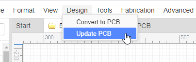
or you can use "Top Menu - Design - Import Changes" at PCB editor.