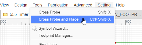
Cross Probe And Place
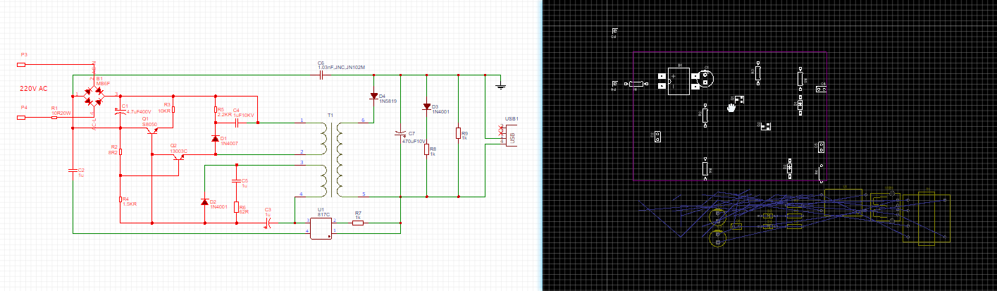
If your schematic have a lot of components, it will be difficult to layout the PCB , so EasyEDA provides a powerful function "Cross Probe And Place".
Top Menu> Tools > Cross Probe And Place
Cross Probe And Place will make the footprints' location match the schematic's parts' location as much as it possibly can.
How to use:
- Convert the schematic to PCB first, and save at current project.
- Frame select the components area by mouse in the schematic, and then click the "Cross Probe And Place", hotkey "CTRL + SHIFT + X".
- The editor will switch to the PCB, and choose the footprints as you selected for waiting for placing.
- Right click to place, and the mouse will keep the drag status, its easy for adjusting the footprints' location.
Notice:
- You need to open PCB first before using this function in the schematic