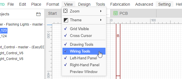
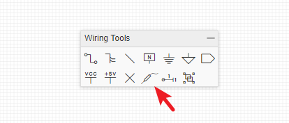
Wiring Tools
If you have hidden your tools , you can open them from here: Top toolbar Top Meun > View > Wiring Tools...
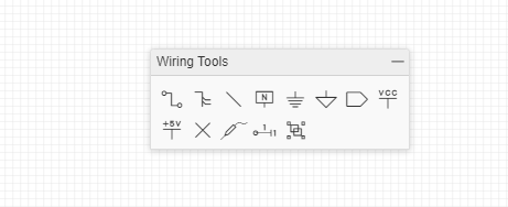
Note: All of the commands in Wiring Tools are electronics related. Don't use a wire when you just need to draw a line, shape or an arrow: use Drawing Tools instead.
Wire
There are three ways to enter the wire mode in EasyEDA.
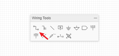
- Click the Wire button from the Wiring Tools palette.
- Press the
Whotkey. - Click on the end of a component pin (where the grey pin dot appears if you select the component):
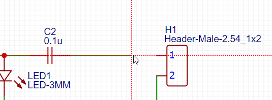
EasyEDA automatically enters Wire mode.
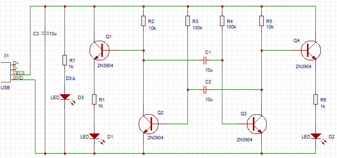
Here is a screenshot of the Astable Multivibrator LED project schematic after wiring:
Moving Components and Wires:
If you place a component, such as a resistor, on top of a wire then the wire breaks and reconnects to the ends of the component.
When moving selected components using the mouse, they will drag attached wires with them (“rubber band”) to some extent but please be aware that the rubber banding feature has some limitations. When moving selected components most wire will move vertically and horizontally. Using the arrow keys will not rubber band. Selected wires do not rubber band.
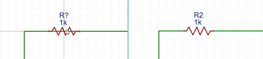
A selected wire can be moved directly by clicking on it using the mouse or by the arrow keys. If a wire is selected by clicking on it using the mouse then green grab handles will appear at the ends and vertices.
Auto adjust connection
If you put a resistor or capacitor on a wire, the wire will auto connect the pins as below:
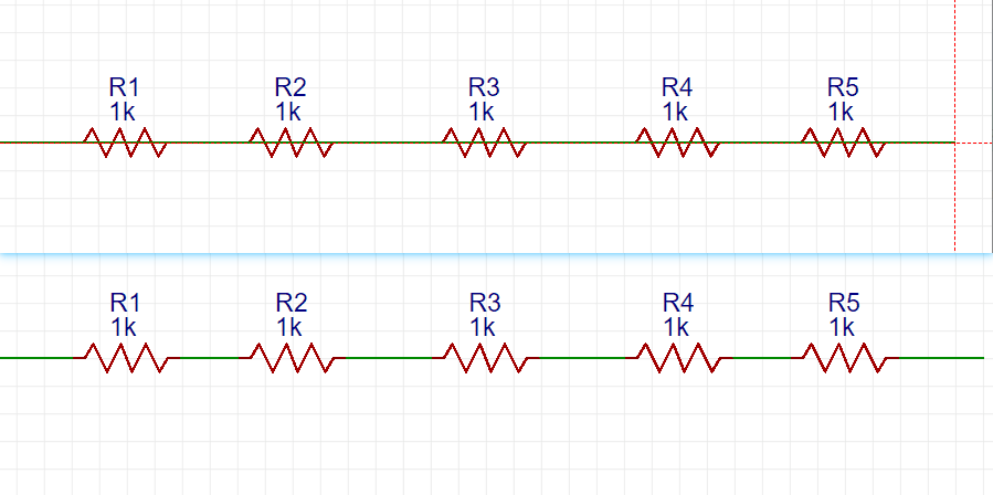
When you want to wiring a series of resistors which are in a row, you can just wire through them, and then you will find they all be connected.
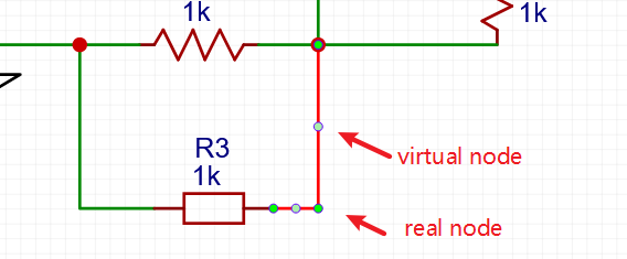
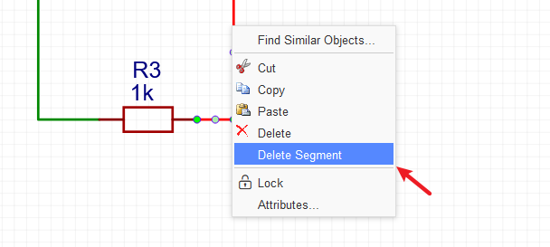
Wire Node
When you click on the wire, you can see the nodes on the wire, where the white is the virtual node, the red is the real node, drag the virtual node to generate the real node, and right-delete the line segment is to delete the line segment between the real nodes.
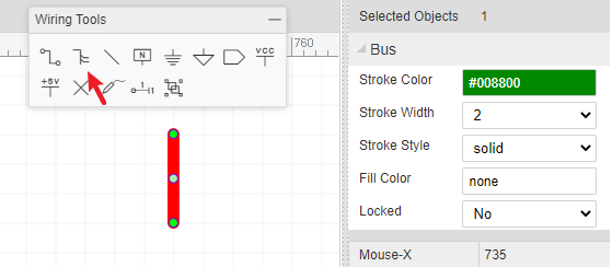
Bus
When you design a professional schematic, perhaps it will use a lot of wires. If you wiring one by one, much time would be wasted, and then you need to use Bus.
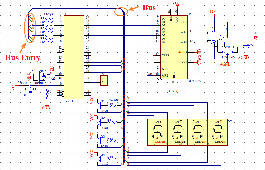
Bus Entry
If you decide to wire with Bus , the Bus Entry must connect to Bus and other nets with wires. such as in the above image.
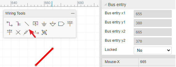
The "Bus" and "Bus Entry" just for the indication, because when you place Bus and Bus Entry, you have to place the netlabel on the Bus Entry dot point.
Net Label
NetLabel can be used to give your wires names to help you find them and identify any misconnections. You can find the NetLabel from the Wiring Tools palette or by using the N hotkey. When selecting the netlabel, you will find its attributes in the right hand Properties panel: 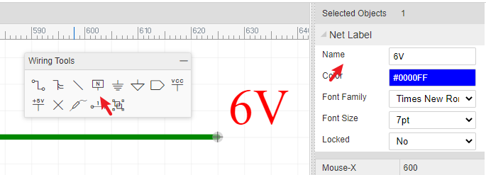
You can change its name and colour. If you only want to change its name, it may be easier to just double click the netlabel.
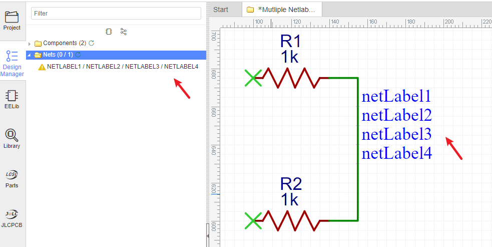
Multi-NetLabels in One Wire
EasyEDA support mutil-netlabel in one wire now.
When you convert the schematic to the PCB, the editor will choose the first netlabel you placed as the net name for this wire, as below NETLABEL1.
Convert to PCB: 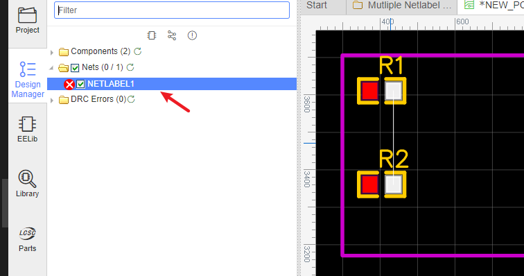
As above image, when you click anyone netlabel's name in the design manager, the wire will be highlighted. 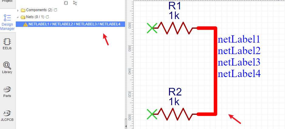
And check the bottom right corner, you will see a warning: 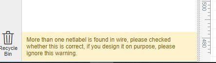
Notice:
- If wire 1 has 3 netlabels A B and C, and wire 2 has netlabel A, then wire 1 and wire 2 are the same net.
- Netlabel/Netflag/Netport/volprobe only support English characters and letters, and Arabic numerals.
- If a part prefix is P1, which has two pins, it will have two nets "P1_1" and "P1_2" by default, if you place a netlabel named P1_1 at other wire which is not connect with P1 pin1, the default "P1_1" will change to "P1_1(1)" for avoid the wrong connection with netlabel "P1_1".
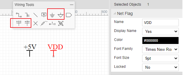
Net Flag
NetFlag is the same as NetLabel, you can find the NetFlag from the Wiring Tools palette or using the Ctrl+G hotkeys for GND or Ctrl+Q for VCC. You can also change its name, for example from +5V to VDD:
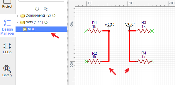
When appear two and more Netflag or Netlabels which are the same name, they will connected with each other.
Wiring Tools palette provides NetFlag: Digital GND, Analog GND, VCC and +5V for your convenience.
Net Port
At EasyEDA, Net Port works like Net Label, it doesn't differentiate the input and output net port. When you don't want to route too many wires, how about trying Net Port :
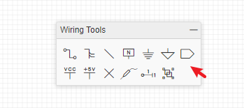
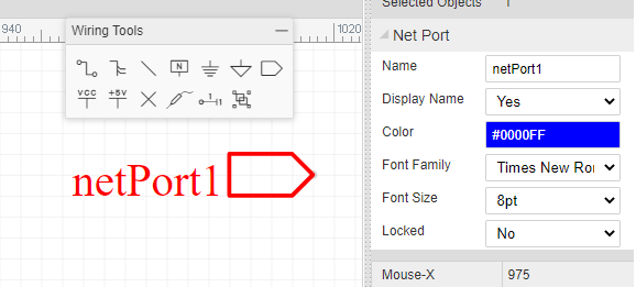
It will make your schematic look more clean, and you just need to set each Net Port a net name.
No Connect Flag
You can find the NO Connect Flag via wiring tool,
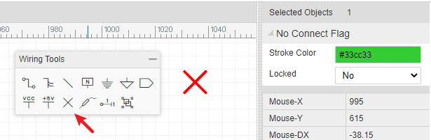
In the below schematic, if you don't add a NO Connect Flag, there is an error flag in the nets collection of the design manager.
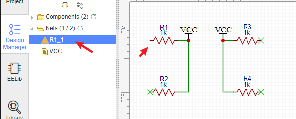
And will show the warning: 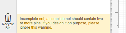
After adding a NO Connect Flag, and then refresh the Nets folder, the error disappears.
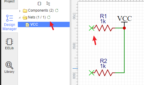
Note: NO Connect Flag suggest placing on the symbol's pin directly, if the pin connected wire, you need to place the No Connect Flag on wire end point, please don't place netlabel on the wire, otherwise, the Design Manager will show error at Nets folder.
Voltage Probe
EasyEDA provides a simulation feature for the schematic. After the simulation is running, you will see the waveform where you placed the voltage probes in the circuit.
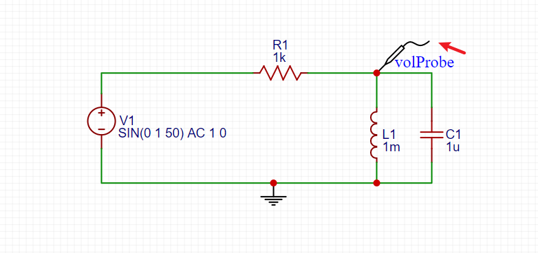
For more detail about the simulation, please check the Simulation section.
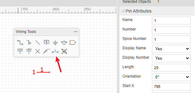
Pin
When you create a new symbol in schematic and schematic lib, you must use Pin to create pins for the new symbol, otherwise your symbol can't be wired with wires.
For more information please refer to the Symbol Library - Create Symbol section.
Group/Ungroup Symbol
On the Wiring Tools palette there is the Group/Ungroup Symbol… button.
Just like the Symbol Wizard, this tool is also for you to quickly create schematic library symbols.
Here's how.
Place Pins and other objects such as rectangle
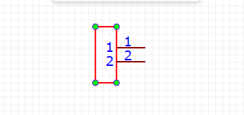
Select them, and click the "Group/Ungroup Symbol" icon
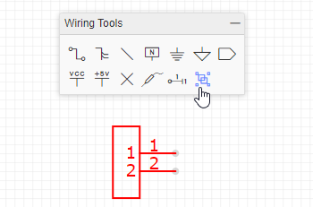
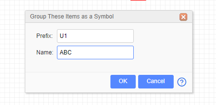
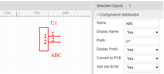
Type the prefix and name, press OK, done. A part is created.
So what does Ungroup do? Try selecting a symbol and then click the Group/ungroup command to see what happens!
Note:
- The symbol you created in the schematic will not be saved in the personal libraries, if you want to use it repeatly, please create a Symbol via: Top Menu - File - New - Symbol.