Create the Schematic Symbol
Create the Schematic Symbol
Using Schematic Symbol Wizard and Group/Ungroup... is a quick way to create schematic symbols but they are placed directly into the schematic that they are built in.
It is possible to reuse them by copying them (CTRL+C hotkeys) from the schematic they were created in and then cross-document-pasting them (CTRL+SHIFT+V hotkeys) into a different schematic but this quickly gets messy if you need to copy symbols that were created in several different schematics.
OK, you could keep copying new symbols into a dedicated “symbol library” schematic sheet to save searching for them but EasyEDA offers you an easier way to create and manage your symbols in a library.
Start a new Schematic Lib as shown below or by doing:
1. File > New > Symbol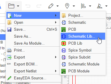 This opens the New SchematicLib symbol editor.
2. Create the symbol
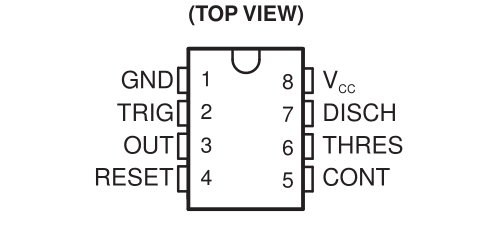
Get the Datasheet For example, using the NE555DR, the datasheet you can refer LCSC: NE555DR. And then create the symbol and place the pins for the library base on the datasheet. This component have 8 pins and names.
Create via Schematic Symbol Wizard
 The more information of Schematic Symbol Wizard please refer next section.
Create by Manually
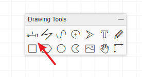
- Draw the shape via the Drawing Tools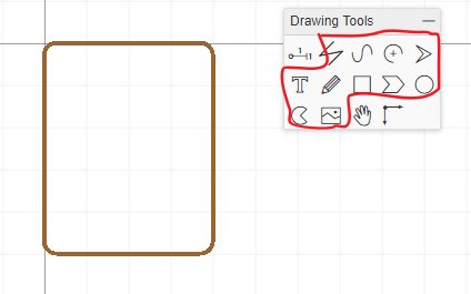 - Place the Pins
 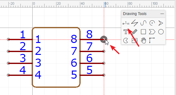 The Pin dot must keep out side as the image indicated, it is connecting with the wires. The more information please refer SchematicLib Attributes - Pins Section.
3. Edit the pin map Via Edit > Pin Map..., change Pin names and Pin numbers. For some complicated IC, will use the alphabet for the pin number. 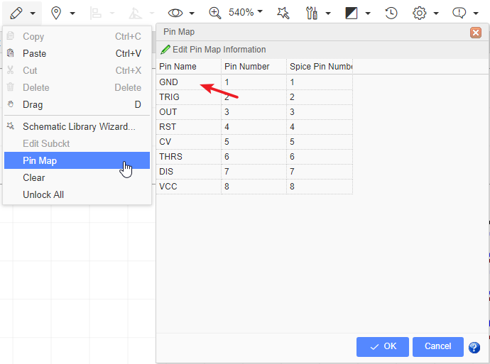
Note: if the pin is hidden, a network will be generated according to the pin name for connection. If it is not necessary, it is recommended not to hide.
4. Modify the Detail such as change Pin length, place text, change Pin color, Pin attributes etc. 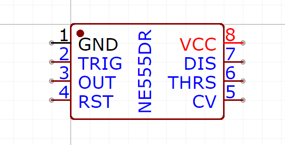
5. Set Costom Attributes You can set the supplier, footprint(Suggested, you must assign the footprint via "Footprint Manager"), Name(Required), Prefix(Required) for it, the more detail of attributes please refer below section: Custom Attributes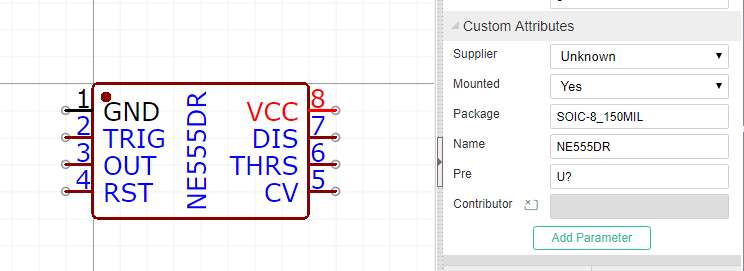
If the schematiclib need to assign the packahe, the Pin number should match the footprint's Pad number. The detail of the footprint assign please refer the Footprint Manager section at previous.
- If the part's property "Convert to PCB" is set as "No", it will not appear at footprint manager.
6. Set the Origin You can via: "Top Menu - Place - Set Canvas Origin - By Center Grid of Symbols" to set the origin.
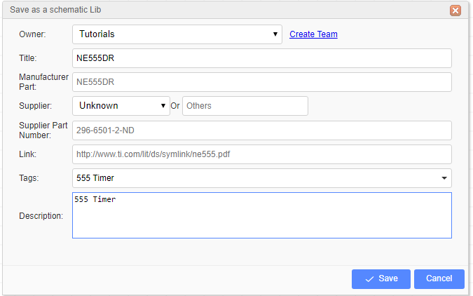
7. Save your SchameticLib You can set this library's owner, datasheet link and tags etc. 
Then a Schematic Symbol is created finish. And the you can find it at "Libraries - SchematicLib - Personl" on the left-hand. 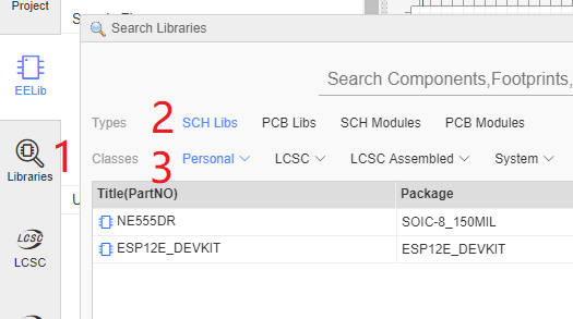
Notice:
- Note the Origin Point. To simplify rotating your symbols when they are placed into the canvas, make sure all of your symbols are created as near as possible centered around that point. Suggesting the first Pin/Pad or its center to be the origin point.
- Please make sure all pins dot are placed on the grid, otherwise, when place the library on the schematic will causing the wiring difficult.
Pin Attributes
Symbols pins are the most important part of any Schematic Lib symbol. They are the things that allow wires to be attached to symbols to connect up your circuit.
You can use the P hotkey to add a Pin or from the Draw Tools pallete:
Before placing it on the canvas, you can use the rotation hotkey or rotate and flip from the menu to rotate it to the right orientation. Make sure the Pin Dot(black dot) is in the right position. The Pin Dot will be used to connect your wires or netlabels. Whenever a PIN is either placed as directly onto the canvas or as part of a symbol, the mouse has to point to the Pin Dot position to automatically start the Wire mode or to join a wire to it.
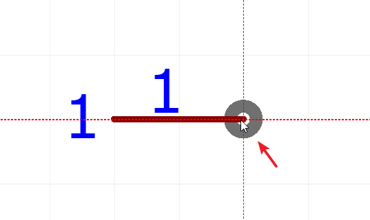
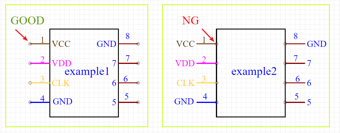
Whenever a Pin is placed as part of a symbol, the Pin dot should be outside of — and pointing away from — the symbol like in example 1(correct position), inside or pointing towards the symbol as shown in example 2(wrong position).
When you select a single Pin, the Pin attributes will be shown in the right hand Properties panel:
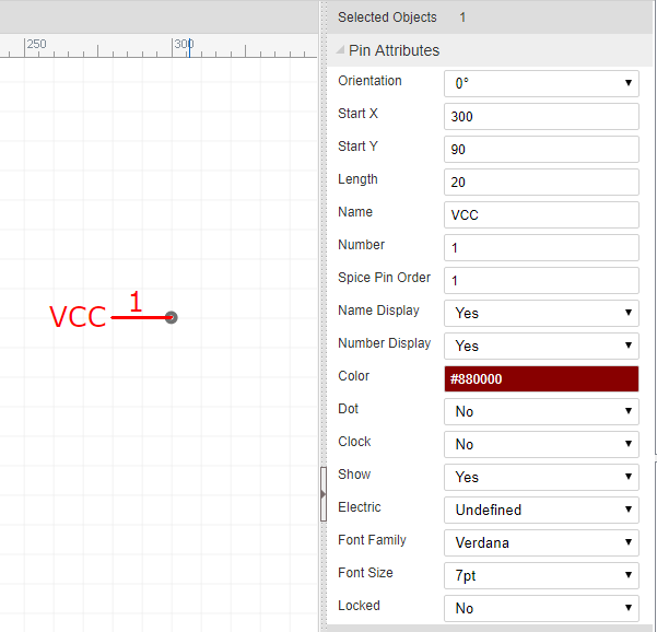
Orientation: 0°,90°, 180° and 270°。If you want to create a 45° pin, you need to set it length as 0, and draw a line with 45°。
Start-X and Start-Y: The pindot position. Sometimes it may be difficult to move the pin to the desired position using the mouse, so you can move the pin via Start-X and Start-Y.
Length: Pin length.
Name: In this example, VCC is the name of the Pin.
Number: In this example, 1 is the number of the Pin. This number is the pin number of the device in a physical footprint.
Note that you can use alphanumeric identifiers such as; A1, B1, C1, A2, B2 and so on as the Number.
Spice Number: These are the pin numbers used to connect your symbol to the corresponding pins defined by the .model or .subckt used to simulate your device. The pin numbers of the simulation model may be different from the physical footprint pin numbers and - unless the model is specifically created to model multiple devices in a single footprint - do not change for different instances of a device in a multi-device footprint. The Spice Pin order must be numerals only.
Name Display: If you don't want to show VCC, switch it to NO.
Number Display: If you don't want to show 1, switch it to NO.
You can adjust the Name or Number position using your mouse but note that rotate and flip applies to the whole pin including the name and pin number; these items cannot be rotated and flipped independently of the pin itself.
Note also that rotate and flip actions do not result in upside down or mirrored pin number or names.
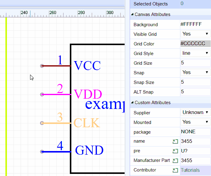
Color: You can set the Pin to different colours, such as PIN3:CLK as orange and PIN4:GND as blue. In this example, the PIN1 is set as color #880000, but it shows as red, because it is selected. After deselecting it, the pin will appear color #880000.
Dot: adds a circle to the inside end of the pin to indicate logical (or analogue) inversion.
Clk: adds a > to the inside end of the pin to indicate that the pin is logical clock input.
Show: YES/NO. Allows you to hide the pin. When set it to NO, this Pin will be hidden when the symbol is placed on the schematic editor canvas, and then create a net which name same as this pin name.
Note that the pin is not hidden here in the Schematic Lib symbol editor canvas because if it was, it would disappear from view and so how would you find it to make it visible again? For the same reason this option has no effect in symbols made using Group/Ungroup…
We may not have thought of everything in EasyEDA but we do try. 😃
Electric: [Undefined, Input, Output, I/O, Power]
EasyEDA provides Electrical Rules Checking (ERC) right now, But you still need to set electric of your Schematic libs.
If you set the PIN as Power and set the pin to be hidden, then the Pin will be connected by Name which is the NetLabel. If the Name is VCC, it will be connected to the net in your circuit with the NetLabel or NetFlag VCC. This is helps to keep the schematic clear and uncluttered when using Multi-part Components.
After created the Lib, use CTRL+S will open the save dialog:
After clicking Save, you will see it appears in Libraries > Symbols > Personal of the left hand Navigation panel. 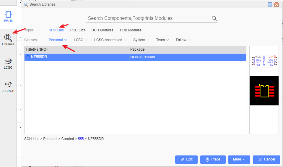
If you want to modify the tag for your new symbol: Libraries > Symbols > Personal > Select New Lib > More > Modify, or right-click new Lib > Modify, if your Lib doesn't have the tags it will appears on All. 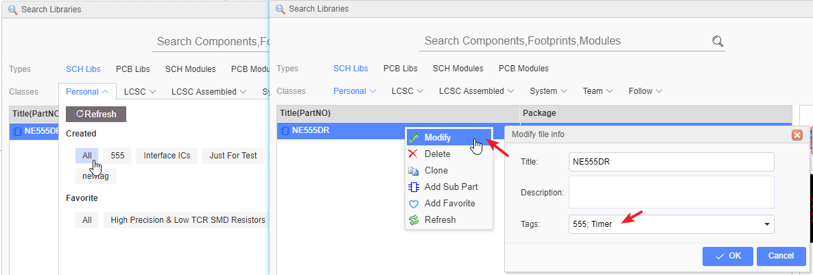
Custom Attributes
In the Schematic Lib editor's canvas Properties panel, you will find a Custom Attributes section:
- footprint
How to change Schematic Symbol's footprint? If you would like to built a PCB, you need to assign a footprint for your Schematic symbol. Although there are other ways to do this in EasyEDA, here is the right place to do it. When you set a footprint , the footprint's pad numbers must match the schematic Lib's pin number, otherwise, when you convert the schematic to PCB , there will miss several nets.
Click in the footprint input box, and the Footprint Manager dialog will open as used to do this task in the Schematic Editor.
The more information please refer to Schematic - Footprint Manager section.
Notie: You have to assign the footprint via the Footprint Manager, otherwise, the Schematic lib will not get the footprint correctly. The footprint is linked with SchematicLib by global unique ID not the title.
- Prefix
The default Schematic symbol Prefix is U? If you create a resistor, you can set the Prefix to R?. It is filled required.
- Name
You can change the schematic lib's name here, it is can be different from the part's file name.
- Contributor
This is your registered user name. When Other EasyEDA's users use your libraries, they will remember your contributions!