Libraries
Commonly Library
That contains ready made symbols for a wide range of components and which can be simulated.
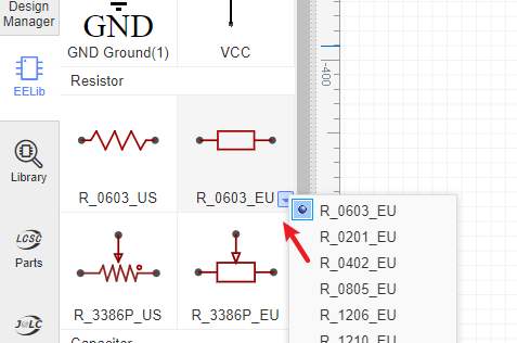
Many of these components have optional US and EU style symbols, we split them, so you can select those you like. Click on the drop down list or right click to popup the context menu, it contains many footprints or parameters. EasyEDA will remember your choices for the next time.
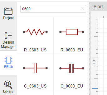
Don't forget to use Filter to locate a component fastly. For example, you just need to type 0603 to find all of resistors:
Library
EasyEDA provide a lot of libraries, you can find them at "Left-hand Panel - Library", hotkey "SHIFT+F", at here you can search library from LCSC, system, user contributed etc.
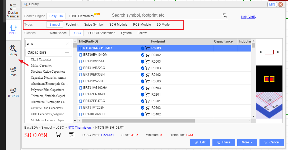
Type
- Symbol: Schematic symbols
- Spice Symbol: Symbols for spice simlation
- Footprint: PCB footprints, PCB pattern.
- SCH Modules: Schematic modules, a part of the circuit design. It can not assign the PCB module, doesn't like the schematic Symbol can assign the footprint . when it be placed on the schematic, it will be separated.
- PCB Modules: As like as Schematic modules.
- 3D Model: It is bind with footprint via "3D Model Manager".
Classes
- Work Space: It include your personal parts and your teams' parts.
- LCSC: EasyEDA online part store LCSC.com parts(Officail Parts). It will add new libraries everyday
- LCSC Assembled: JLCPCB Assembled parts. All JLCPCB assembly parts will contain a SMT icon, that means this part can be JLCPCB assemble.
- System: EasyEDA system parts, it comes from open source libraries, such as Kicad libraries, company public libraries, user contributions.
- Follow: If you follow a user at EasyEDA(You can follow a user at him/her user page), you can view and use his/her libraries.
- User Contributed: When you searching a part, maybe you can find it at this class. At EasyEDA, all libraries are public. the detail you can refer at: Contribute
We add an "JLCPCB Assembled" Components option of the Parts, It's easy to choose which component can be assembled by JLCPCB. Yes, JLCPCB will provide the assembly service. the more information please refer at: How to order a SMT order
Search Engine - EasyEDA
Simply type your part number or symbol's name to Search. before searching, you must choose the "Type" first.
and then click the "Table of contents" to open the categories list to choose your components.
From there you can scroll up and down to browse parts from each category.
If you know the component's name Suppose you want to find the MAX232 (which converts signals from an RS-232 serial port to signals suitable for use in TTL compatible digital logic circuits). Simply type
Max232into the Search box and press Enter: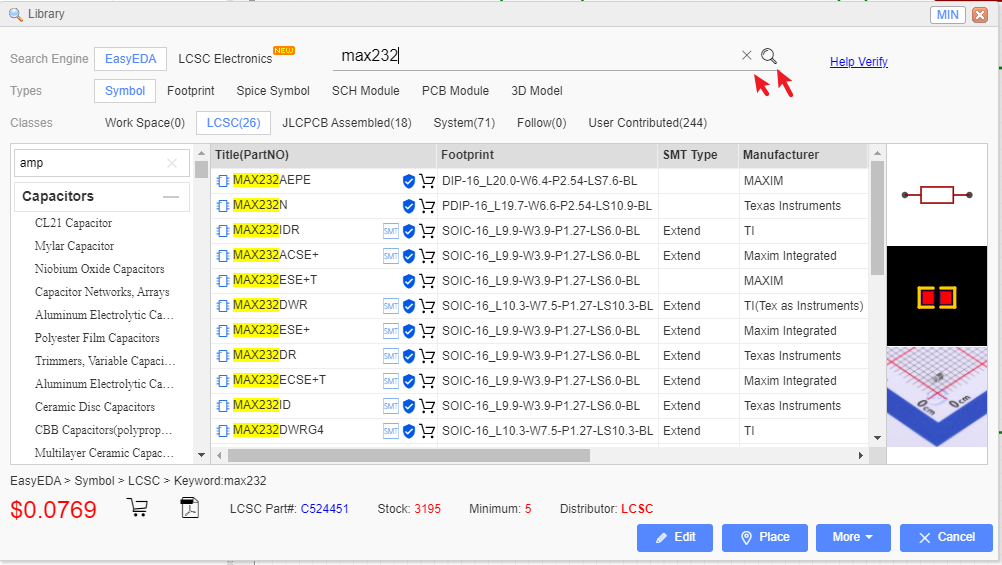
If you don't know the component's name For example, you want to find a resistor which value is 1kohm, footprint is 0603, at Libraries you can follow below steps: - 1.Choose the library type - 2.Typing the keyword such as
1k 0603- 3.Click the search button - 4.Select the class you which is wanted of the result - 5.If you don't need the search you need to remove all the search keywords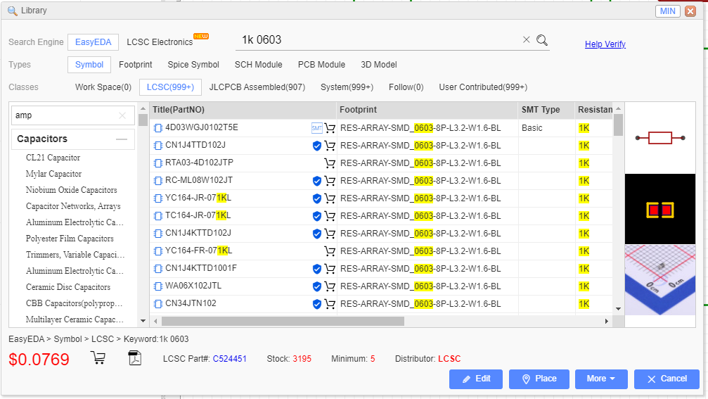
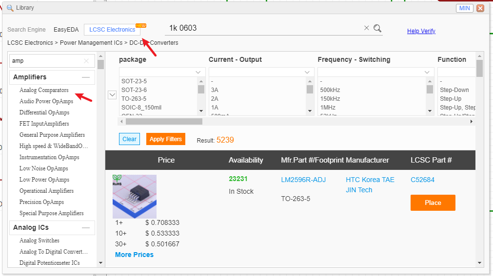
Search Engine - LCSC Electronics
When you want to find some parts by clearly parameter, you should try "Search Engine - LCSC Electronics", it all most same as LCSC.com.
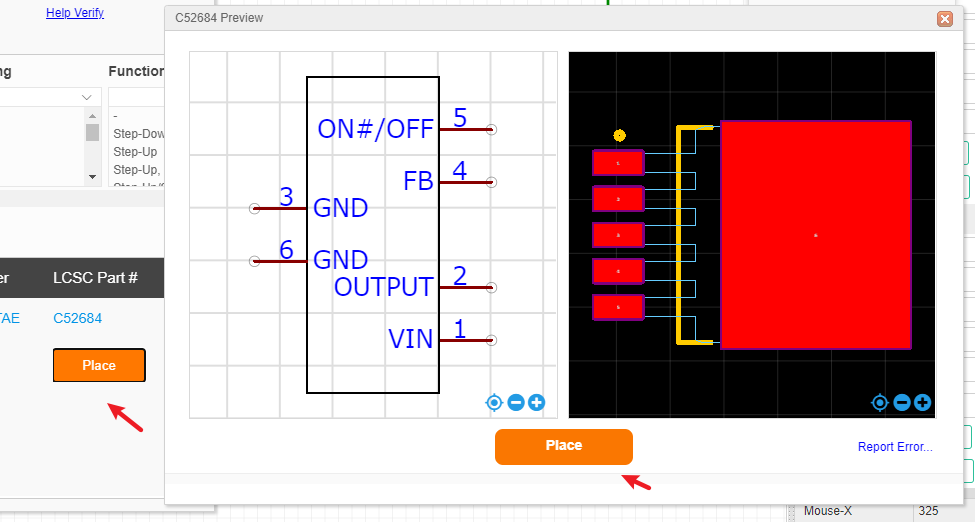
When you find out part, and you can place into the schematic:
Notice:
- The subpart can not be preview at Preview dialog window, if you find out this, you need to change to "Search Engine - EasyEDA" to place this part.
Max and Min mode
If you want to place without close the "Library" dialog, you can change dialog mode to Min mode, just click the Min button at the top-right corner. 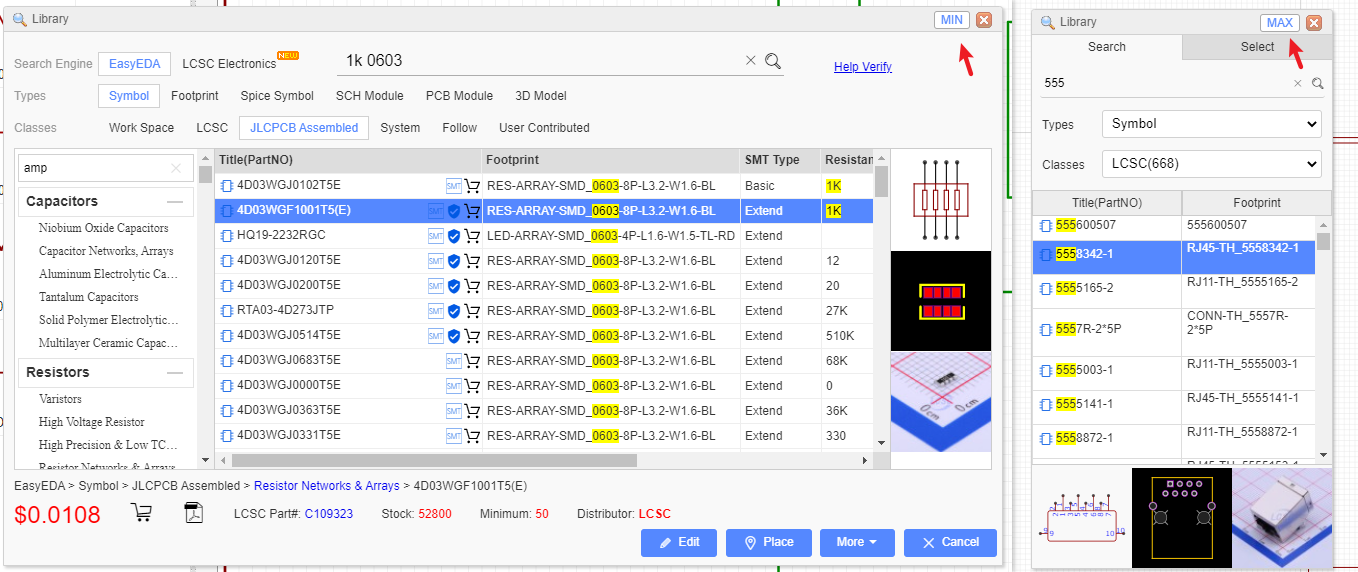
Operations
When you hover the mouse over the picture of the Schematic symbol or PCB footprint, you will find a toolbar with "Edit", "Place", "More" buttons.
Place:
For parts you use infrequently, you don't need to Favorite them; just Place it into your canvas directly. Or you can double click the library to place.
Note:
EasyEDA supports multi-documents so please make sure that you are placing the part into the right (active) document. The active document is the one with the highlighted tab.
You can't place a Schematic symbol into a PCB file, or a PCB Footprint into a schematic.
EasyEDA will try the best to make sure the library is correct, but it still has incorrect parts, if you find any incorrect parts please let us known. suggested order a sample first before ordering a big order.
Edit:
If you want to create your own version of a symbol or footprint then you can open an existing part from the library to use as a template, edit it and then save it to your local Work Space library in Library of the Navigation Panel.
More:
We can't promise that every component in the library is free of errors so please check all symbols and footprints carefully before you commit to a PCB order.
If you do find a mistake in a component, please use the Report Error, so that we can fix it.
Components with sub parts (multi-device footprints).
When you find a component with sub-parts, you can't Place or Edit it, but you can Favorite and Clone it as your own part, which you can then edit.
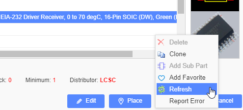
Right-Click
When you right-click the part list, you can edit its tags, add favorite etc. 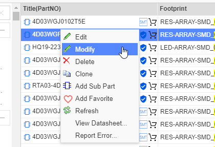
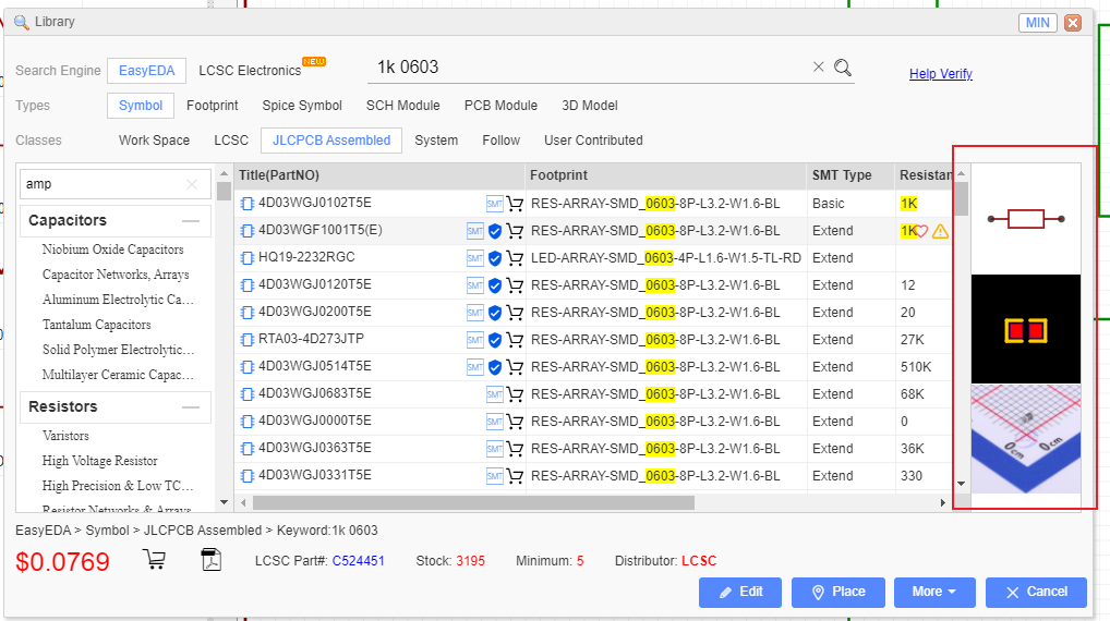
Preview Image
Every library when you click, you can check its preview image, such as symbol, footprint, production picture. Click the the image you can open it quickly.
Placing Components
Find the component which you plan to place to your schematic at "Libraries", then move your mouse to the canvas and left click. If you want to add more, just left click again. To end the current sequence of placements, right click once or press ESC. 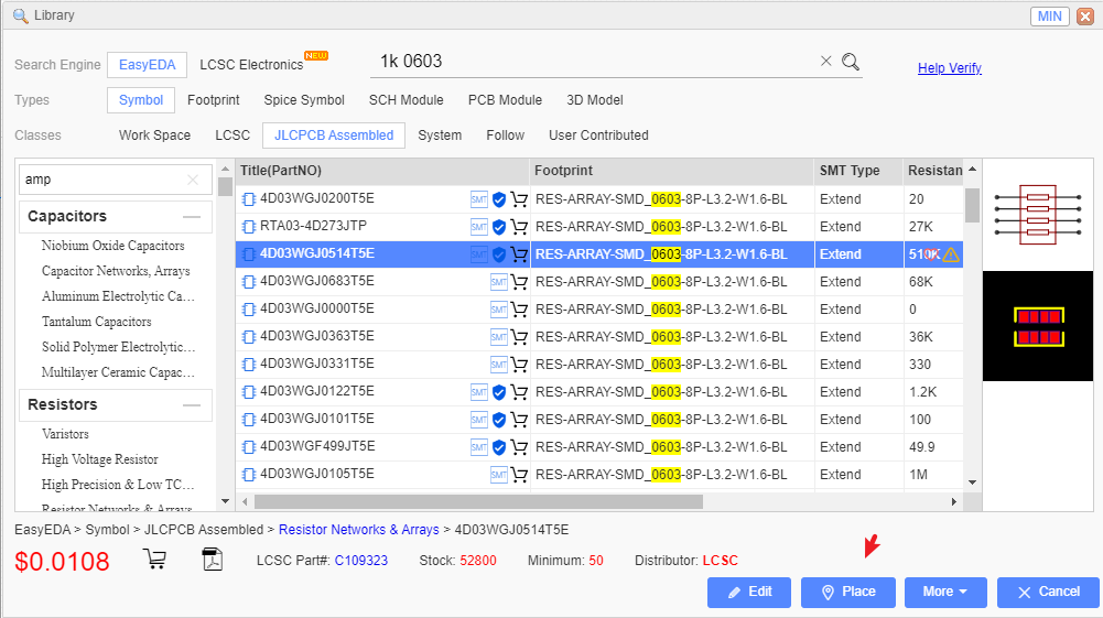
Don't try to Drag and Drop a component to the canvas EasyEDA team thinks that Click-Click to place components will be easier to use than a Click-Drag mode.
Multi-part Components
The number of pins on some components can be quite large. That's why it's easier to divide such a component into several parts or functional blocks, it calls multi-parts or subparts.
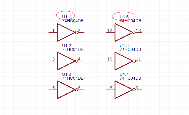
As a simple example, there are six gates in the 74HC04 Hex Inverter component. To avoid clutter in the schematic, GND and VCC pins of such components are usually served by a separate part of the component. This is really convenient as it doesn't interfere the working process with logical parts. The NetLabel names of VCC and GND Pin are usually hidden.
When placing the 74HC04 on a schematic, it will look like the screenshot below.
Note: The component Prefix will be in form of: U?.1, U?.2 etc.
If you click the father-part and place on the schematic, the remaining subparts will be placing one by one, if you click the one of the subpart, you will placing U1.1, U2.1, U3.1 etc.
How to create multi-part(subpart) please refer Create Symbol
Starting with v6.4.20.8, the editor enables the historical versioning mechanism for schematic and footprint libraries. When a symbol or footprint library is saved, a new history record will be generated each time it is saved, and when the library is placed on the canvas, the latest historical version of the library will be used. For example, MAX232 schematic library and footprint SOP-8, when the MAX232 schematic library is bound with SOP-8, it is placed in the schematic diagram and converted to PCB. At this time, the version used by the SOP-8 of the PCB is the historical version that was placed in the schematic diagram at that time. , if you edit the footprint library SOP-8 again and add one more pad, the schematic diagram will be transferred to a new PCB again, and the original footprint will still be used. If you want to use the new version footprint, updates the corresponding component at schematic design menu. This design ensures that the version used at the time is not affected by subsequent footprint modifications, ensuring that the version placed at that time is always used. If it is a schematic diagram drawn before v6.4.20.8, the latest version of the footprint will still be taken directly when transferring or updating the PCB, because the old file placement device does not record the historical version at that time. This mechanism does not currently support private deployment versions.
Schematic Symbol Wizard
How many times have you hit a schematic capture roadblock because you couldn't find a component symbol?
Well, in EasyEDA that would be never because the Schematic Symbol Wizard provides a quick and easy way to create a general schematic library symbol.
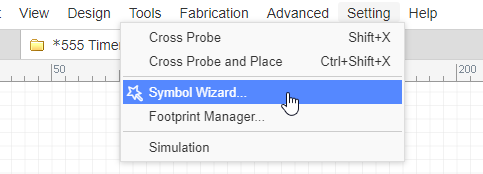
Via: Top Menu > Tools > Symbol Wizard in a new schematic symbol or sheet document.
The professional function please refer at Schematic Symbol Wizard