Export PCB
Export PCB in PDF/PNG/SVG
Exporting a PCB design or footprint from EasyEDA is very similar to exporting a Schematic or a Symbol.
Use: File > Export > PDF/PNG/SVG…
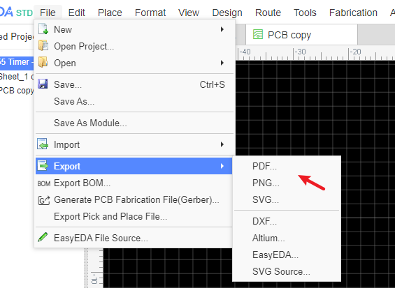
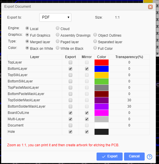
This dialog will open:
You can choose to export in PDF, PNG or SVG format.
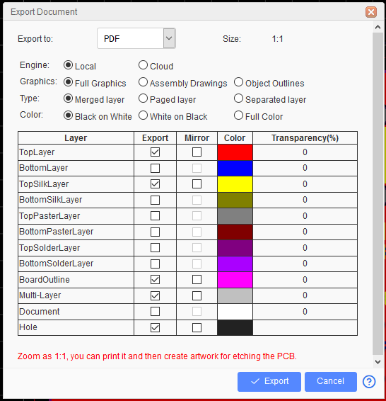
Note: _The PDF size is zoom as 1:1 with PCB. _
Export to: Support export to PDF, PNG, SVG. To print the PCB as 1:1 you should choose PDF.
Engine:
- Local: PDF generated by Editor
- Cloud: PDF generated by Cloud Server, this feature is planned to be removed in the future.
Graphics: - Full Graphics: All graphics and objects will be exported.
Assembly Drawings: This exports only component prefixes, locations, holes, etc. This is used for parts assembly.
Object Outline: This only exports the objects outlines, such as Pad and silkscreen outlines.
Type:
- Merged layer: All selected layers will be merged into one page.
- Paged layer: All selected layers will be separate pages in a single file.
- Separated layer: All selected layers will be exported into separate files contained in a ZIP file.
Color: You can choose "Black on White", "White on Black", "Full Color".
Layer: You can select to print individual layers or selected layers merged into a single file.
Mirror: It is also possible to mirror selected layers so that the bottom layers are shown in easily readable orientation. This is recommended when all your selected layers are bottom ones.
If EasyEDA PDF does not satisfy your requirements, please let us know. 
If you generated the Gerber file, you can use the Gerbv application to easily export the PDF file.
Use: Gerbv
Export PCB in Altium Designer Format
The more information please refer at Export Altium
Download PCB
Please refer to Export EasyEDA Source
Print PCB and Etching
EasyEDA doesn't support directly printing the PCB, instead export to PDF and then print.
If you don't want to order your PCBs from EasyEDA then maybe - for single and double sided PCB designs - you can try using some homemade PCB tech:
http://hackaday.com/2012/12/10/10-ways-to-etch-pcbs-at-home/
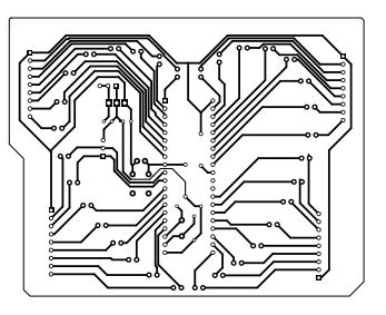
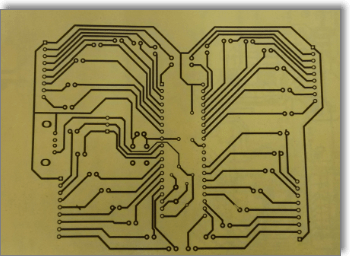
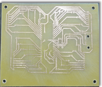
So, here's how you can print your PCB layer by layer and then etch it onto a PCB.
Step 1) Export it to PDF, Using: File > Export > PDF…
Note: Make sure the Colour is Black on White Background.
For the bottom layer, select the mirror option on export if needed.
If you have routed PCB tracks on the top layer you will also need to export that layer. Etched PCBs generally need to use the mirror export printing option.
Step 2) Open the pdf file in a viewer
Step 3) Print it to paper
Step 4) Copy it to the copper
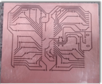
Step 5) Etch it
Step 6) Drill it
Step 7) Get your soldering iron out!