Editor FAQ
Please spend a few minutes reading this FAQ, it will save you lots of time getting started with EasyEDA.
Tutorial
Download for PDF
Details
Video Tutorials
Details
Ask for Help
Details
Update Records
Details
Schematic
If I update the schematic, how do I then update the PCB?
Details
Using: "Menu - Design - Update PCB".
Alternatively, you can import changes from the schematic from within the PCB Editor:
How to rename a Sheet/Page or modify description.
Details
In this menu, there is a Modify option, so you can rename your files. Double click or right-click the sheet tab can change the sheet title too. 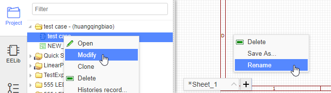
What is the unit of the schematic sheet? How to change schematic unit?
Details
The basic unit of the schematic sheet is the pixel. 1 pixel is about 10mil (0.001 inch) but please note that this use of the pixels as a unit in a schematic is just for reference.
For a complex project, I want to split the schematic over several sheets. Does EasyEDA support hierarchy?
Details
EasyEDA don't support hierarchy, but support multi-sheets。 Please check out this link https://docs.easyeda.com/en/Schematic/Multi-Sheet/index.html
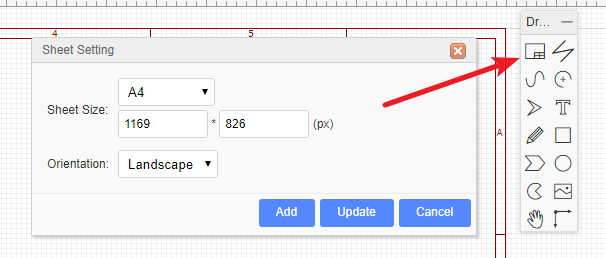
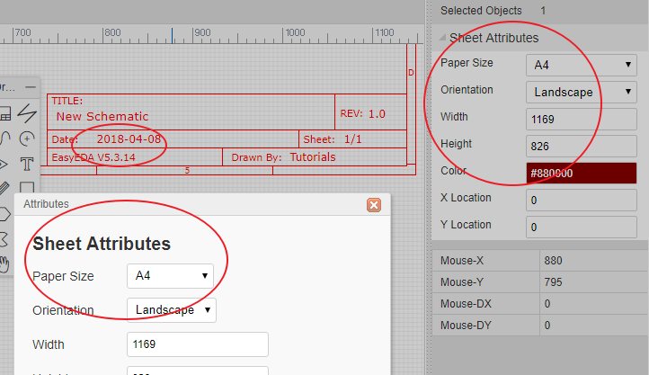
How to change the sheet size and modify the design information.
Details
To change the sheet size, move the mouse anywhere over the lower right area of the drawing border or frame until the whole border highlights red and then right-click on it. Paper size and orientation can then be changed in Sheet Attributes in the right hand panel.
To modify the design information, left-click on the relevant blue text in the lower right area of the drawing border or frame to change it in Text Attributes in the right hand panel. Double left-clicking the blue text will allow you to type new information directly into the field.
How to indicate low electronic level in the Schematic Pin or Netlabel
Details
You can add a # characater in the pin name/netlabel last text. You can use symbols that you are familiar with. You do not have to add a line above the netlabel name.
I can't convert schematic to PCB. Why is this?
Details
- You have not set the right footprints for your components.
- Prefix Conflict Error
- Invalid footprints
PCB
How to solve the PCB very slow issue
Details
Because of v6.3 add two features:
- All objects support show the ratlines which are containing nets;
- Solve bottom layer pads will cover top copper issue. These features will make editor slower than before.
There are some methods to try to improve:
- Via Tools - Design Rule, disable real-time DRC
- Via Settings - PCB settings, disable Add Teardrop Automatically
- Via Settings - PCB settings, disable Net Highlighting While Coursor Hover the Track
- Via Settings - PCB settings, disable The Track's Routing Follows Component's Rotation
- Via Settings - PCB settings, disable Rebuild Plane Automatically, and using copper area instead of inner plane layer
- Via Settings - PCB settings, set Canvas Zoom Effect as Speed Priority
- Hide ratline layer before move footprints at PCB
- Check footprints which have a lot pad's, and the pads are polygon type, please modify them as Retangle or Oval
- Suggest PCB doesn't over 300 footprints, Pads and Vias no more than 1500
How to change the Units of PCB from mil to mm or inch.
Details
There is an option for that in PCB canvas attributes: 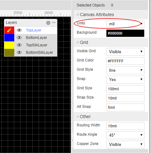
How to pick and move the components on the PCB canvas quickly.
Details
Before routing the PCB, the components need to be positioned in suitable places on the PCB. In the PCB Editor, it can sometimes be quite difficult to select components by clicking on the silkscreen outline or the pads. To select and move them more easily, please use drag mode (Hot Key D) or click the Move icon in the PCB Tools toolbar: 
How to add test point in schematic or PCB?
Details
Schematic: You can place a single pin connector from Commonly Library, and then update its footprint.
PCB: You can place a top/bottom layer pad , and then route it with track.
Can I create a PCB without creating schematic?
How to add more fonts for PCB.
Details
You can refer to Text of PCB section.
How to insert an Image/Logo to PCB.
Details
You can refer to Image of PCB section.
How to insert a DXF as board outline.
Details
You can refer to Import DXF File of Import section.
How to create non rectangular pcb outline such as round?
Details
You can import a DXF file for the board outline. For a round board outline, you can use an arc to do that, you just need to change to the board outline layer, then draw 1 arc like in the image below (need to adjust a bit later), you can use lines and arcs to create complex board outlines.
How to add a slot and cut out.
Details
Please use solid region https://docs.easyeda.com/en/PCB/PCB-Tools/index.html#Solid-Region
Or draw a track and right-click it, use the "Convert to Board Cutout" option.
How to measure dimensions on a PCB.
How to add more layers.
Details
Click the layer options button, then tick the extra layers in the dialog that opens. https://docs.easyeda.com/en/PCB/Layers-Tool/index.html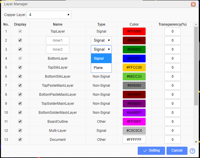
How to add solder mask aperture.
Details
It is possible to get boards with the copper exposed so that you can apply a layer of solder over those tracks to further increase their current carrying capacity. In this case, you need to add solder mask over a copper (copper area, track, solid region). EasyEDA will add solder mask for pads automatically. Sometimes however, you may need to add an aperture in the solder mask to expose and area of copper.
First, add a top or bottom solder mask layer, as required.

Next, draw a region in the solder mask layer over a copper item as illustrated in the image below. This in effect draws an aperture in the solder mask so that the copper item inside the region, in this case the track, will be not be covered by the green film of solder mask.
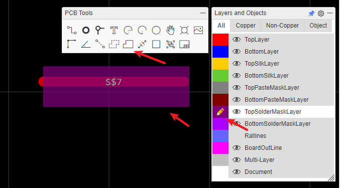
A common mistake is to just draw a solder mask, without a copper area, like the track pointed to by the yellow arrow. That is incorrect and does not produce the desired result.
Or you can click the track, and then click the Expose Copper button at the right-hand panel. 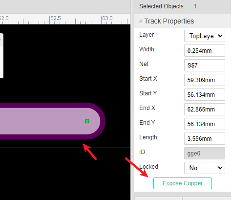
How do I set the dimensions of my PCB in the layout?
Details
PCB's dimension/size depends on the board outline, you can create your board outline, please refer to Board Outline of the PCB section.
My PCB is complex, how can I be sure that I have routed all of the tracks?
Details
Please refer to Design Manager of PCB section.
I need to start my layout again, how can I remove all of the tracks?
Details
You can use "Menu - Route - Unroute All" and "Menu - Edit - Global Delete".
How to put a component on the bottom layer?
Details
There are two ways to do this.
- If your active layer is the bottom layer, then every component you place will be placed on the bottom layer automatically.
- You can place a component then select it and change its layer attribute to
Bottom layerin the right hand panel.
How to panelize the PCB
Details
Please refer at PCB: Panelize
What does Warning copper area do not allow self intersection
Details
Please refer at Forum: What does Warning copper area do not allow self intersection
Library and Parts
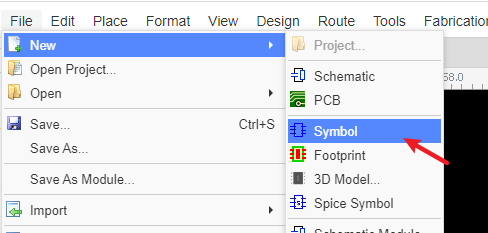
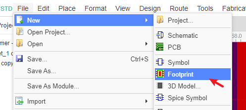
How to create a schematic symbol library.
File > New > Symbol
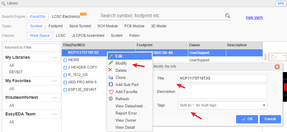
How to tag my schematic library symbol.
After creating the library and saving, you can add a tag for it, and you can add and edit the tag at "Library":
How to create sub parts for multi-part components.
In personal part list, Right click the part then select Add Sub Part from the menu that opens: 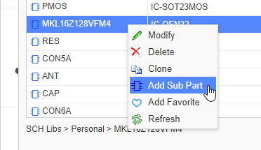
How to change the footprint for a component.
https://docs.easyeda.com/en/Schematic/Footprint-Manager/index.html
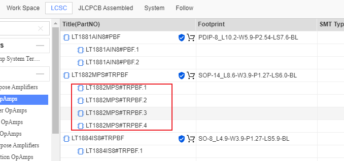
How to add sub parts to a schematic.
You can add sub parts to a schematic one by one but please note that the sub parts prefix must be in the form of U1.1 U1.2 etc, and not U1.A U1.B.
How to create a PCB footprint.
How to change a component's footprint?
please refer at Footprint Manager
How to find components/parts/libraries?
The component search function has been significantly improved to make finding part symbols and footprints quicker and easier. Press SHIFT+F or click on the Libraries icon on the left navigation panel:
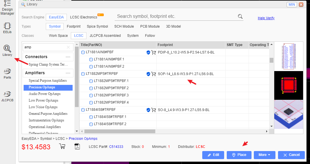
In the new components dialog, it is easy to select the right components via tags and you can set tags for your own components.
Fabrication and Order
How to Order PCB
Before ordering, please check this Gerber first: https://docs.easyeda.com/en/PCB/Gerber-Generate/index.html#Gerber-View
Visit and login at https://jlcpcb.com/quote
Add this Gerber file(compressed file) on the page and type the order options
Save to Cart, and then submit the payment
If you want to combine the components order with the PCB order at https://lcsc.com , please refer: https://support.lcsc.com/article/24-do-you-offer-combine-shipment-with-pcbs
please refer at Order PCB
How export BOM and order parts?
please refer at Export BOM
Import and Export
How to import Alitum/Eagle/Kicad File?
Please refer at Import Altium Designer
Can I export my design?
Yes, you can export your design as EasyEDA format or Alitum Designer format. Please refer at:
How to export or print the schematic or PCB?
please refer at Export
Save and Backup
Where are my files?
Your files are stored on EasyEDA servers, so you can access them anywhere and share them with your partners.
if you using EasyEA desktop client, you can set the runing mode as "Project Offline Mode", it will save your project to local.
How to save my file to the local?
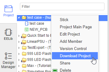
You can download the project via :
- Right-click project and download;
- Download the EasyEDA Source
- Export to Altium file Export: Export Altium
I don't like others seeing my design. How can I stop that happening?
Set your project as Private. For extra security you can even save your work locally.
as above to save your file to locad as EasyEDA format.
Is EasyEDA safe?
There are no absolutely secure things in the world but even if you have the misfortune - as happened to one of our team - of losing one laptop and having two hard drives break, EasyEDA will try to protect your designs in following ways:
- We utilize SSL throughout the entire domain EasyEDA.com. Secure Socket Layer (SSL) technology encrypts all data transferred between your computer and our servers. Your data is for your eyes only.
- You can save your files locally.
- Multiple copies of every file are saved in your local database.
- EasyEDA servers backup your designs frequently.
What if EasyEDA cannot become self sustaining and has to close down?
We promise to do our best to ensure that neither of these things will happen; we have spent so much of our time to get to this point. We promise that if we cannot make enough money out of EasyEDA to keep it alive or to fund further development, we will not simply abandon our baby or our community but we will consider donating the code to the Open Source Community to let them build on our efforts. There are no companies who can stay forever, so if a time comes when we have to close down, we will follow the steps below:
- Give our users six months warning prior to closure;
- Ensure all our users can backup their designs;
- Ensure that user's designs can be exported to some other EDA tools, such as Kicad, Altium Designer and others.
- Package our codes, so that users can install an EasyEDA in their own OS (Windows, Linux, Mac). Users can then build their own cloud EDA.
- Upload our codes to github.com and make them open source.
So, nothing will be lost and our users can continue to enjoy an awesome web based EDA tool that lets them stay in charge of their designs: anywhere, anytime and on any OS.
How to backup my project?
Please refer at: Saving Your Work Locally
Spice Simulation FAQ
EasyEDA's main target is schematic and PCB, not simulation. EasyEDA only support simple schematics simulation.
How to set the resistance of a resistor
You can use the name attribute. Just set the name or double click the value text.

Where Can I find the Probe/voltage probe?
Voltage probe 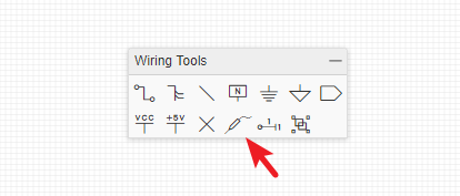
Why I can't simulate my schematic
EasyEDA only has very few simulation models, EasyEDA is powered by LTSpice, please check LTspice to know what can be simulated.
How to ask for help and get an answer
[Must read] How to ask for help and get an answer
Others
Can I use EasyEDA in my company?
You are free to use EasyEDA for individuals, business and education. If you add our Logo and link on your PCB/Video we will appreciate.
What happens if EasyEDA service is offline for some reason?
EasyEDA can be run as an offline application. You can export your design first, when the service back, you can import the design and save to EasyEDA server.
Or you can use EasyEDA desktop client "Project Offline" mode.
How to find the list of hotkeys.
Please refer at Introduction: Shortcut Keys
Why does EasyEDA focus on Cloud based EDA?
EasyEDA is built for people who like to work anywhere, who like to build projects together with other team members, who like to share their projects, who like something that operates like a github for hardware design. The only way to meet these needs is to build a Cloud version EDA.
How can I work if there is no internet?
Although most of the time there are ways to access the internet easily and cheaply there may be times when, for whatever the reason, internet access is simply not possible. For times like this, EasyEDA is working to provide a desktop client soon.
Does EasyEDA have a desktop version?
Yes, please refer at: https://easyeda.com/page/download
Which Browser is best for EasyEDA?
The latest Chrome and Firefox. If you are restricted to using other browsers, it would be better to download the EasyEDA desktop client.
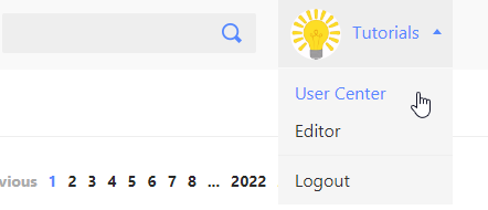
How to go to your dashboard.
In the User Center, you can check all your Projects, Modules, Libraries and Friends, Messages etc.
There are two ways to arrive there.
From the Editor, you can click on user logo:
From the homepage, you can click My Projects:
How to delete a project.
Select it and right click to open a context menu, like the image below. 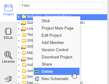
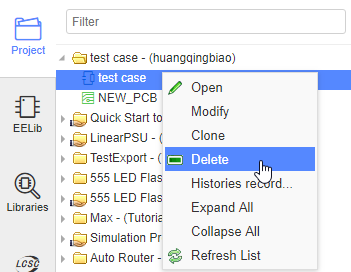
How to delete a schematic or PCB.
Select it and right click to open a context menu, like the image below.
How to share a project with others.
- Make your project public.
- To share a project privately with only selected collaborators via: Add Member
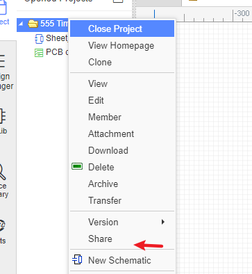
How to find the version history of schematics and PCBs.
The version history of your EasyEDA schematics and PCBs can be accessed by right-clicking on the file you wish to query to open the context menu as shown in the image below:
Then click on the version number that you wish to view.
Note: saving a previous version will restore that version to being the current version of the file.
Does EasyEDA canvas use the Cartesian coordinate system?
Yes and no.
It uses X and Y coordinates where the horizontal X coordinate is positive to the right of the origin and negative to the left but the vertical Y coordinate is positive below the origin and negative above it.
Actually, we think our coordinate system is not very good but it is hard to change.
How to update editor to latest version and how to remove editor cache?
please refer at: How to Update
Essential checks before placing a PCB order
Please refer Essential checks before placing a PCB order
Keep in Mind
After the first save of any file, EasyEDA will back up all saved files automatically under the Version Control. If you want to back up your files locally, you can download a copy of the whole project or of individual files in a project in EasyEDA Source (JSON) format:
 and File > EasyEDA File Source > Download
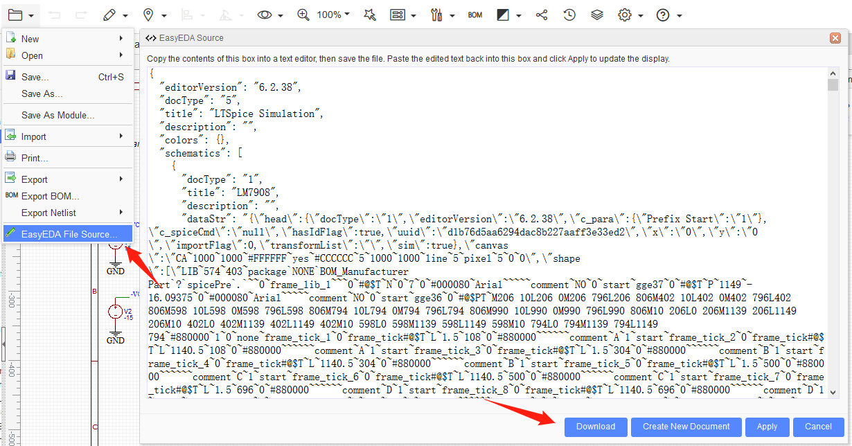
If you need help, you can contact us email or ask via our Support Forum; we will respond ASAP.